PCB automatic line moving processing method
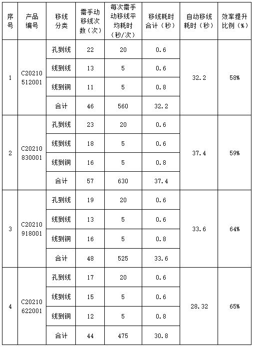
A line processing and automatic technology, applied in the direction of printed circuits, electrical components, printed circuit manufacturing, etc., can solve the problems of human error, affecting customer satisfaction, customer complaints, etc., to improve the efficiency and quality of data processing, improve accuracy. The effect of turnover rate and large income
- Summary
- Abstract
- Description
- Claims
- Application Information
AI Technical Summary
Problems solved by technology
Method used
Image

Examples
Embodiment
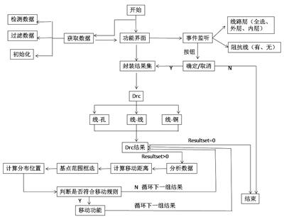
[0037] A method for automatic wire transfer processing of PCB, comprising the following steps:
[0038] S1. Get all circuit layers and drilled via layers:
[0039] S11. Adjust the direction of all the lines of the circuit layer;
[0040] S12. Perform simple attribute judgment on the acquired circuit layer and drilled layer;
[0041] S13. Line attribute screening: keep the lines of the line layer, copy the pads that are not in contact with the drilled holes to the new temporary layer, copy all the copper attribute D codes to the new temporary layer, if the impedance line attribute is defined, the impedance Copy the line to the new temporary layer;
[0042] S14. Automatically filter out the holes, use a copper D code temporary layer, contact the drill layer, and filter out the drill holes that are in contact with the copper skin;
[0043] S15. Encapsulate wire, pad, hole and copper data.
PUM
 Abstract
Description
Claims
Application Information
 - Generate Ideas
- Intellectual Property
- Life Sciences
- Materials
- Tech Scout
- Unparalleled Data Quality
- Higher Quality Content
- 60% Fewer Hallucinations
Browse by: Latest US Patents, China's latest patents, Technical Efficacy Thesaurus, Application Domain, Technology Topic, Popular Technical Reports.
© 2025 PatSnap. All rights reserved.Legal|Privacy policy|Modern Slavery Act Transparency Statement|Sitemap|About US| Contact US: help@patsnap.com