Photonic crystal double-band-pass filter

A dual-band-pass filter and photonic crystal technology, applied in the field of integrated optics, can solve the problem of little research work on photonic crystal dual-band and multi-band-pass filters, and achieve the effect of high integration and strong anti-interference.

Pending Publication Date: 2022-08-02
SHANGHAI INST OF MICROSYSTEM & INFORMATION TECH CHINESE ACAD OF SCI
View PDF0 Cites 0 Cited by
  • Summary
  • Abstract
  • Description
  • Claims
  • Application Information

AI Technical Summary

Problems solved by technology

The development of all-solid-state, miniaturized, and low-power dual-passband filters has become an important research topic in the field of future communication technology. However, there are not many researches on photonic crystal dual-passband and multi-bandpass filters. Technology needs to be solved urgently

Method used


Image

  • Photonic crystal double-band-pass filter
  • Photonic crystal double-band-pass filter
  • Photonic crystal double-band-pass filter

Examples


Embodiment Construction

[0045]The embodiments of the present invention are described below through specific specific examples, and those skilled in the art can easily understand other advantages and effects of the present invention from the contents disclosed in this specification. The present invention can also be implemented or applied through other different specific embodiments, and various details in this specification can also be modified or changed based on different viewpoints and applications without departing from the spirit of the present invention.

[0046] When describing the embodiments of the present invention in detail, for the convenience of explanation, the cross-sectional views showing the device structure will not be partially enlarged according to the general scale, and the schematic diagrams are only examples, which should not limit the protection scope of the present invention. In addition, the three-dimensional spatial dimensions of length, width and depth should be included in...


PUM


Abstract

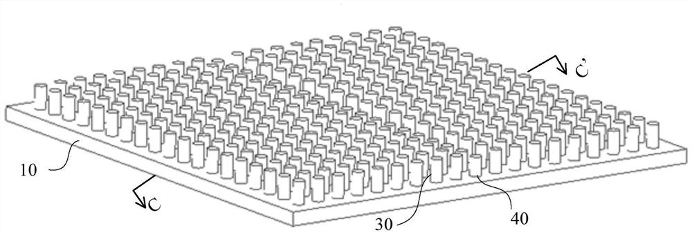
The invention provides a photonic crystal double-band-pass filter which comprises a first metal plate, a second metal plate, metal columns and defect metal columns, the first metal plate and the second metal plate are correspondingly arranged, and the metal columns are arranged between the first metal plate and the second metal plate in a two-dimensional periodic mode. Two opposite ends of the metal columns are respectively contacted with the first metal plate and the second metal plate to form a metal column array; the height of the defective metal columns is smaller than that of the surrounding metal columns, the defective metal columns comprise first defective metal columns and second defective metal columns which have different cross sectional areas so as to form defective sub-periodic structures, and the defective sub-periodic structures are arranged in the metal column array in a two-dimensional periodic mode. The invention provides a photonic crystal double-band-pass filter which can be used for 6G communication and optical communication in the future, and fills the blank in the field.

Description

technical field [0001] The invention belongs to the field of integrated optics and relates to a photonic crystal double bandpass filter. Background technique [0002] In 1969, Dr. Miller of Bell Labs proposed the concept of integrated optics. The main research goal of integrated optics is to integrate bulky free-space optical systems on the same substrate. Among them, the size of the integrated optical device varies with different frequency bands. For example, the millimeter wave frequency band is generally in the order of millimeters, and the terahertz (THz) frequency band is mainly in the order of micrometers. The integrated optical device has the advantages of low power consumption and small size, and at the same time, because it is in a relatively closed environment after integration, the interference of external electromagnetic radiation is very small. Under the background that integrated circuits are constrained by Moore's Law and their prospects are limited, optoele...

Claims


Application Information

Patent Timeline
Patent Type & Authority Applications(China)
IPC IPC(8): H01P1/20
CPCH01P1/20
Inventor 王长郑永辉谭智勇张真真曹俊诚
Owner SHANGHAI INST OF MICROSYSTEM & INFORMATION TECH CHINESE ACAD OF SCI
Why Eureka
Try Eureka