Method and apparatus for minimizing dopant outdiffusion in gate structure
A gate structure and dopant technology, applied in the direction of electrical components, transistors, circuits, etc., can solve the problems of reducing the amount of dislocations, reducing retention time, damage, etc., and achieve the effect of reducing outward diffusion
- Summary
- Abstract
- Description
- Claims
- Application Information
AI Technical Summary
Problems solved by technology
Method used
Image
Examples
Embodiment Construction
[0031] The invention will now be described in detail with reference to several illustrative embodiments shown in the accompanying drawings. In the following description, numerous specific details are set forth in order to provide a thorough understanding of the present invention. It will be apparent, however, to one skilled in the art, that the present invention may be practiced without some or all of these details. In other aspects, some well-known structures and steps are not described for brevity.
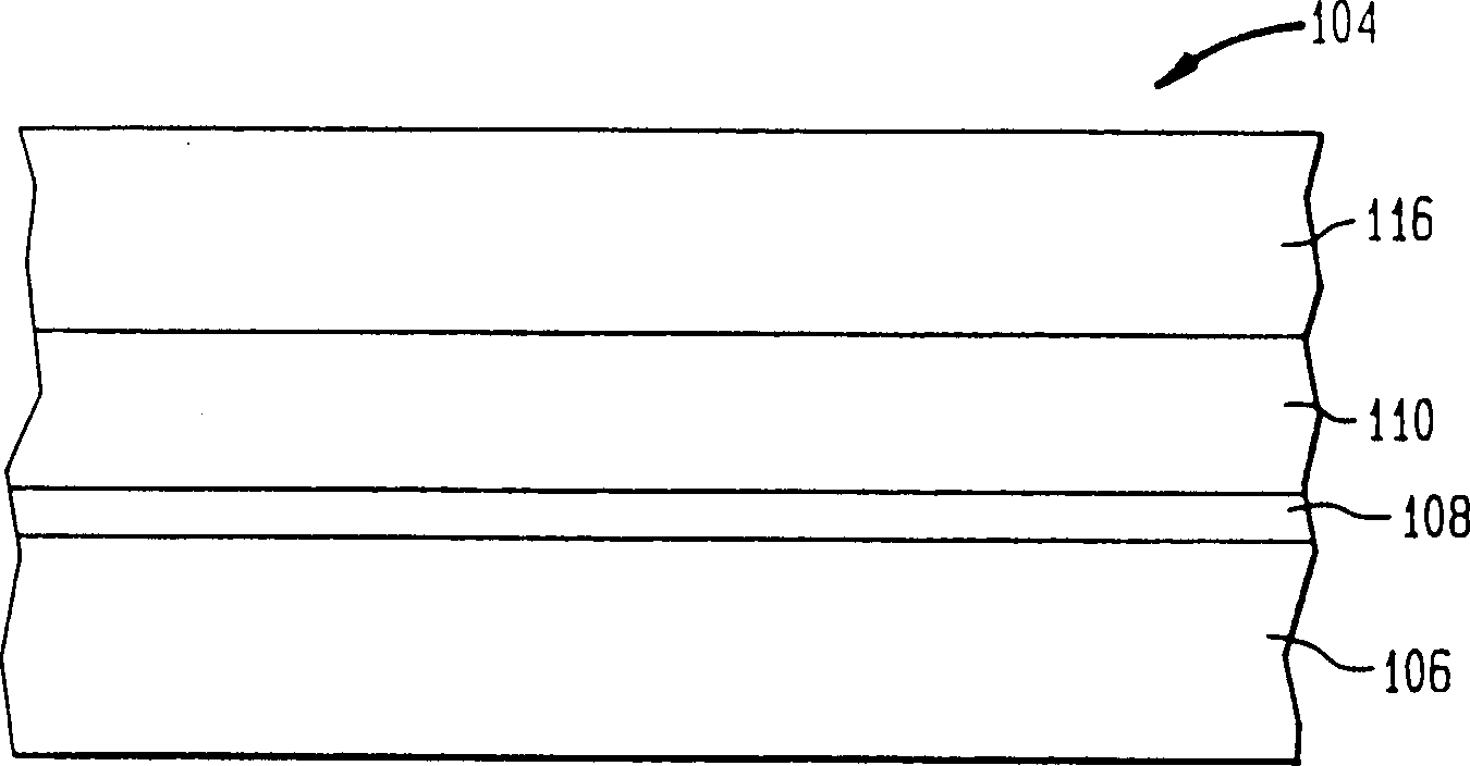
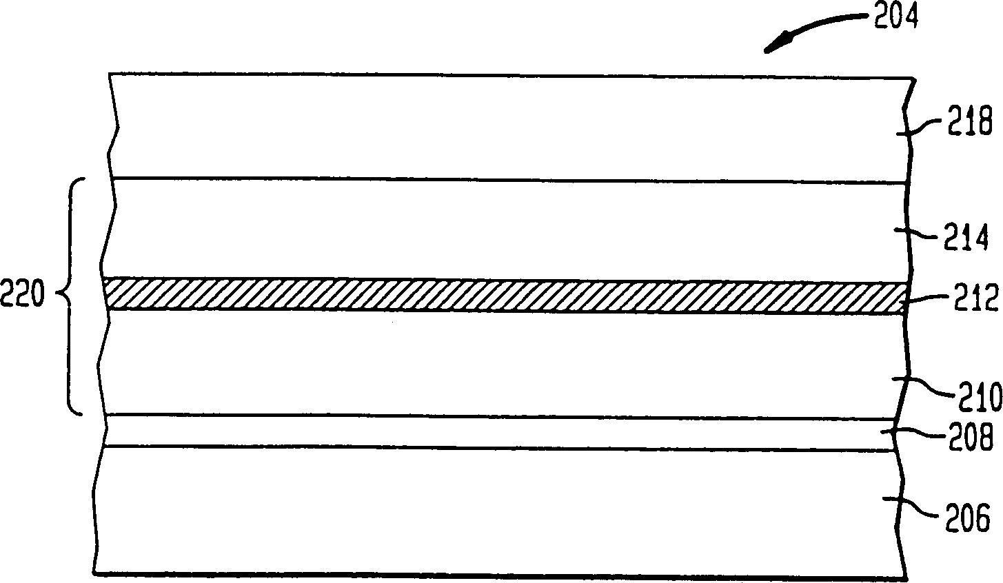
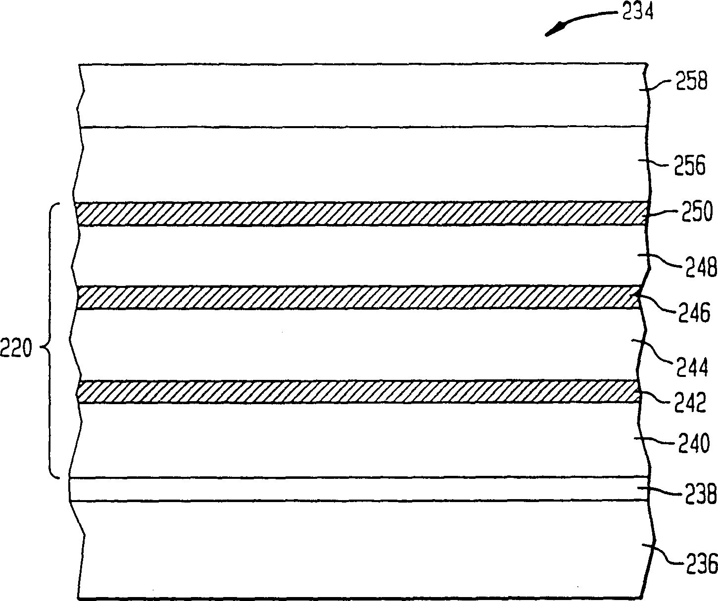
[0032] In order to reduce the amount of outdiffusion of dopants into the silicide layer in the gate structure (eg, a gate interconnect structure) during annealing, according to one aspect of the present invention, in the gate structure, a barrier layer to prevent the diffusion of dopants. Figure 2A is a diagram showing a first gate structure in an integrated circuit with a barrier layer according to an embodiment of the present invention. It must be understood that this is o...
PUM
 Abstract
Description
Claims
Application Information


