Flip-chip semiconductor device with stress absorption layer made of resin and its manufacture method

A stress-absorbing, semi-conductor technology, applied in semiconductor/solid-state device manufacturing, semiconductor devices, semiconductor/solid-state device components, etc.

Inactive Publication Date: 2005-09-28
RENESAS ELECTRONICS CORP
View PDF1 Cites 2 Cited by
  • Summary
  • Abstract
  • Description
  • Claims
  • Application Information

AI Technical Summary

Problems solved by technology

Multiple flexible conductive member injection openings

Method used


Image

  • Flip-chip semiconductor device with stress absorption layer made of resin and its manufacture method
  • Flip-chip semiconductor device with stress absorption layer made of resin and its manufacture method
  • Flip-chip semiconductor device with stress absorption layer made of resin and its manufacture method

Examples


Embodiment Construction

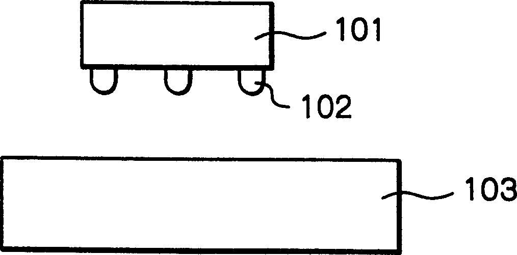
[0035] Before describing the preferred embodiment, reference will be made to Figure 1A , 1B , 1C explains the prior art flip chip type semiconductor device.

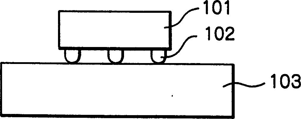
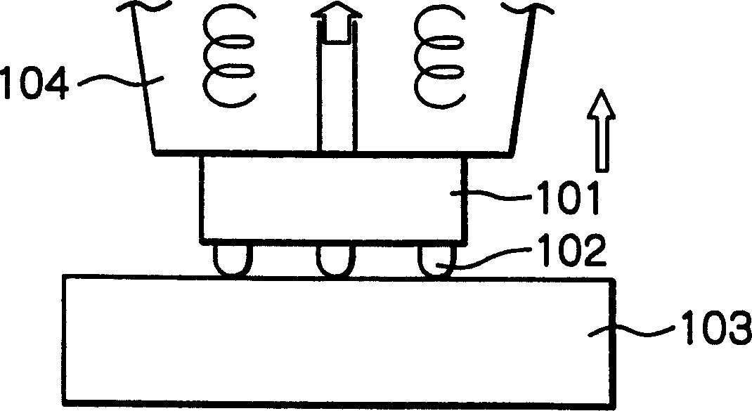
[0036] Figure 1A , 1B , 1C are schematic diagrams explaining a conventional method of mounting a flip-chip type semiconductor device on a mother board.

[0037] first reference Figure 1A , a flip-chip type semiconductor device 101 having metal bumps 102 and a motherboard 103 having electrodes (not shown) corresponding to metal bumps 102 are prepared. Note that the motherboard 103 is prepared by the user.

[0038] next step, refer to Figure 1B , the semiconductor device 101 is mounted on the motherboard 103 . Note that if the metal bump 102 is a solder ball, the solder ball is reflowed at one of the predetermined temperatures and soldered on the mother board 103 . In this case, due to the difference in thermal expansion coefficient between the semiconductor device 101 and the motherboard 103 , stress strain is ge...


PUM


Abstract

In a flip-chip type semiconductor device, a plurality of pad electrodes are formed on a semiconductor substrate. An insulating stress-absorbing resin layer made of thermosetting resin is adhered to the substrate as a composite layer in conjunction with a first conductive layer and has openings corresponding to the pad electrodes. A plurality of metal bumps are formed on the conductive layer.

Description

technical field [0001] The present invention relates to a flip-chip type semiconductor device and its manufacturing method, and in particular to reducing stress strain in a flip-chip type semiconductor device. Background technique [0002] In recent years, flip-chip type semiconductor devices have been developed to meet the demands of higher performance, smaller and lighter size, and higher speed of electronic equipment. [0003] Generally speaking, a flip-chip semiconductor device with metal bumps is directly mounted on a motherboard with corresponding metal bump electrodes. That is, if the metal bumps are solder balls, the solder balls are reflowed and soldered to the motherboard. In this case, due to the difference in thermal expansion coefficient between the semiconductor device and the motherboard, stress strain is generated, which will degrade the reliability of the semiconductor device. It will be explained in detail later. [0004] To minimize the differences in t...

Claims


Application Information

Patent Timeline
Patent Type & Authority Patents(China)
IPC IPC(8): H01L23/52H01L21/3205H01L21/56H01L21/60H01L23/12H01L23/29H01L23/31H01L23/485
CPCH01L2924/01015H01L2224/0231H01L2924/01023H01L2924/01046H01L2224/0233H01L2924/0105H01L2924/01082H01L2924/01004H01L2224/02333H01L24/94H01L2924/01018H01L2924/09701H01L2224/13144H01L2924/01029H01L2924/00013H01L24/12H01L2224/0401H01L2924/01028H01L24/11H01L2924/014H01L2924/01013H01L23/293H01L2924/01024H01L2924/0103H01L2224/274H01L24/03H01L2224/1134H01L2924/01047H01L2924/01079H01L2924/01007H01L23/3171H01L2924/01068H01L24/13H01L2924/01005H01L2924/01033H01L2924/01006H01L2924/01074H01L2924/01078H01L2924/10253H01L2924/01014H01L2924/01058H01L2924/01075H01L2224/13111H01L2924/12042H01L2924/14H01L2924/00014H01L2224/13099H01L2924/00H01L23/12
Inventor 本多广一
Owner RENESAS ELECTRONICS CORP
Why Eureka
Try Eureka