Lutetium disilicate blended submicron imaging fluorescent sreen and its preparing method

A lutetium disilicate and phosphor screen technology is applied in the field of doped lutetium disilicate submicron imaging phosphor screens and their preparation, which can solve the problems of long light decay time, easy deliquescence of thin films, low coupling efficiency and the like, and achieve high X-ray absorption. coefficient, high quality single crystal film, good optical properties

Inactive Publication Date: 2007-04-04
SHANGHAI INST OF OPTICS & FINE MECHANICS CHINESE ACAD OF SCI
View PDF4 Cites 0 Cited by
  • Summary
  • Abstract
  • Description
  • Claims
  • Application Information

AI Technical Summary

Problems solved by technology

[0003] SCF phosphor screens such as CsI(T1) in the prior art, Ce:YAG / YAG and Ce:LuAG / YAG have the following disadvantages: (1) CsI(T1) and Ce: effective atomic number and density of YAG crystals are very small ( Y eff They are 54.1 and 32 respectively, and the density is 4.52g / cm 3 and 4.55g / cm 3 ), therefore, their absorption conversion efficiency for X-rays is low
(2) CsI(Tl) film is easy to deliquescence, and its light decay time is long (600ns), which is not suitable for fast real-time micro-X-ray imaging; (3) Although Ce:LuAG has a large effective atomic number and high density ( Y eff = 58.9, density = 6.67g / ce 3 ), but its light output is small (3000Ph / MeV), and the lattice mismatch between LuAG and YAG as the substrate is relatively large, which is not conducive to growing high-quality single crystal thin films on the substrate, which will Can seriously affect the optical performance of fluorescent screen; (4) there is afterglow phenomenon in the used scintillator of prior art; device and Si array peaks correspond to 600-1000nm)

Method used


Image

  • Lutetium disilicate blended submicron imaging fluorescent sreen and its preparing method

Examples


preparation example Construction

[0041] The preparation method of the doped lutetium disilicate submicron imaging phosphor screen includes the following steps:

[0042] (1) Raw material equipment:

[0043] ①According to the chemical formula (Ce x M z Re y Lu 1-x-y-z ) 2 Si 2 O 7 , And select x, y, z, equipped with polycrystalline materials;

[0044] ②According to the following components, select the ratio and equip the flux raw materials:

[0045] Composition wt%

[0046] PbF 2 50-60

[0047] PbO 10-20

[0048] PbO 2 Or Li 2 Mo 2 O or K 2 Mo 2 O 7 20-40

[0049] ③According to polycrystalline raw material: flux raw material=10-40wt%, determine the weight percentage of the above-mentioned raw materials;

[0050] (2) Weigh the raw materials according to the weight percentage determined in step (1) above;

[0051] (3) Preparation of lutetium disilicate substrate: lutetium disilicate is oriented and cut into substrate wafers (Lu 1-y Re y ) 2 Si 2 O 7 (0≤y≤0.3) for large-area seed crys...

Embodiment 1

[0063] Example 1: (Ce 0.005 Lu 0.995 ) 2 Si 2 O 7 / Lu 2 Si 2 O 7 Flashing screen

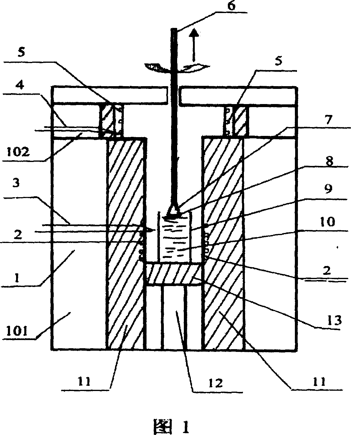
[0064] The selected resistance heating liquid phase epitaxy furnace is shown in Fig. 1, and the crucible 9 in the main furnace 101 is a platinum crucible. According to the above preparation process, the polycrystalline raw material (Ce 0.005 Lu 0.995 ) 2 Si 2 O 7 With cosolvent (PbF 2 :PbO:PbO 2 =55wt%: 15wt%: 30wt%) by weight percentage is (Ce 0.005 Lu 0.995 ) 2 Si 2 O 7 / (PbF 2 -PbO-PbO 2 )=0.10 to weigh the raw materials, a total of 500g, mix well and put them into the platinum crucible 9 of φ80×50mm; the size of φ30×0.03mm, the crystal plane direction is (010) Lu 2 Si 2 O 7 The substrate 8 is placed in the jig 7, and the jig 7 is loaded into the bottom end of the rotating pull rod 6, and the positions of the crucible 9 and the substrate wafer 8 are adjusted to be coaxial, and both are in the center of the main furnace body 101; 101 is heated to 1200°C, the raw materials and flux are melted into ...

Embodiment 2

[0066] Example 2: (Ce 0.001 In 0.1 Lu 0.899 ) 2 Si 2 O 7 / (In 0.1 Lu 0.9 ) 2 Si 2 O 7 Flashing screen

[0067] Will (In 0.1 Lu 0.9 ) 2 Si 2 O 7 Polycrystalline material and cosolvent Li 2 Mo 2 O 7 By weight percentage (Ce 0.001 In 0.1 Lu 0.899 ) 2 Si 2 O 7 / Li 2 Mo 2 O 7 =0.40, weighing a total of 500g of each raw material, the size is φ20×0.03mm, the crystal plane direction is (001) (In 0.1 Lu 0.9 ) 2 Si 2 O 7 The substrate 8 is placed in the jig 7, and the jig 7 is loaded into the bottom end of the rotating pull rod 6, and the positions of the crucible 9 and the substrate wafer 8 are adjusted to be coaxial, and both are in the center of the main furnace body 101; 101 is heated to 1200°C, the raw materials and flux are melted into a saturated solution 10, and after a constant temperature of 1200°C for 5 hours, the rotating lifting rod 6 is gradually lowered so that the substrate wafer 8 is 3mm away from the saturated liquid surface, and then the (Ce 0.001 In 0.1 Lu 0.899 ) 2 Si 2...


PUM

PropertyMeasurementUnit
thicknessaaaaaaaaaa
thicknessaaaaaaaaaa
thicknessaaaaaaaaaa

Abstract

The invention is a doped lutetium disilicate submicron imaging fluorescent screen and its preparing method, adopting a heating-resistance liquid phase epitaxy (LPE) furnace to grow a doped lutetium disilicate flicker film on a lutetium disilicate substrate to make it, and its structure expression is (CexMzReyLu1-x-y)2Si2O7 / (Lu1-yRe)Si2O7, where 0.001<=x<=0.01, 0 <=y<=0.3, 0.001<=z<=0.01, Re stands for one or multiple of Sc, Er, La, Ho, Dy, Yb, Yt, Gd, In, etc, and M stands for Eu or Tb. It can be widely applied to the ray detection fields such as scientific research, medical treatment, industrial nondestructive detection, geological exploration, security inspection, national defence, etc.

Description

Technical field [0001] The invention relates to a sub-micron imaging phosphor screen, in particular to a doped lutetium disilicate sub-micron imaging phosphor screen and a preparation method thereof, in particular to the use of liquid phase epitaxy technology in undoped lutetium disilicate single crystal (Lu 1-y Re y ) 2 Si 2 O 7 (Where 0≤y≤0.3, Re represents one or more of Sc, Er, La, Ho, Dy, Yb, Y, Gd or In) on the substrate (thickness of about 10 microns-2 mm) Grow a layer of doped lutetium disilicate single crystal film (Ce x M z Re y Lu 1-x-y-z ) 2 Si 2 O 7 (Where M represents one of Eu or Tb), so as to prepare a fluorescent screen that can be used for X-ray submicron imaging (Ce x M z Re y Lu 1-x-y-z ) 2 Si 2 O 7 / (Lu 1-y Re y ) 2 Si 2 O 7 , (0.001≤x≤0.01, 0≤y≤0.3, 0.001≤z≤0.01), this kind of fluorescent screen can be widely used in scientific research, medical treatment, industrial non-destructive testing, geological prospecting, security inspection and national defense and...

Claims


Application Information

Patent Timeline
Patent Type & Authority Patents(China)
IPC IPC(8): H01J1/62H01J9/20C09K11/79
Inventor 赵广军严成锋徐军庞辉勇介明印何晓明夏长泰
Owner SHANGHAI INST OF OPTICS & FINE MECHANICS CHINESE ACAD OF SCI
Why Eureka
Try Eureka