

Method and system for polishing semiconductor wafers
A semiconductor and crystal technology, applied in the field of semiconductor processing, can solve the problems of limited number of polishing pad polishing cycles, time-consuming processing, uncertainty in the number of test wafers, etc.
- Summary
- Abstract
- Description
- Claims
- Application Information
AI Technical Summary
Problems solved by technology
Method used
Image

Examples
Embodiment Construction
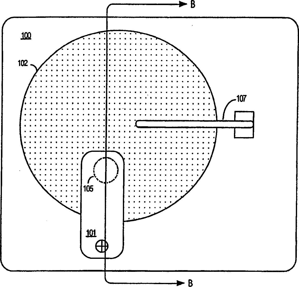
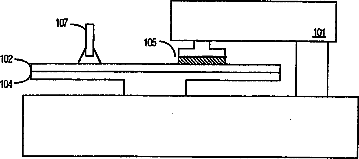
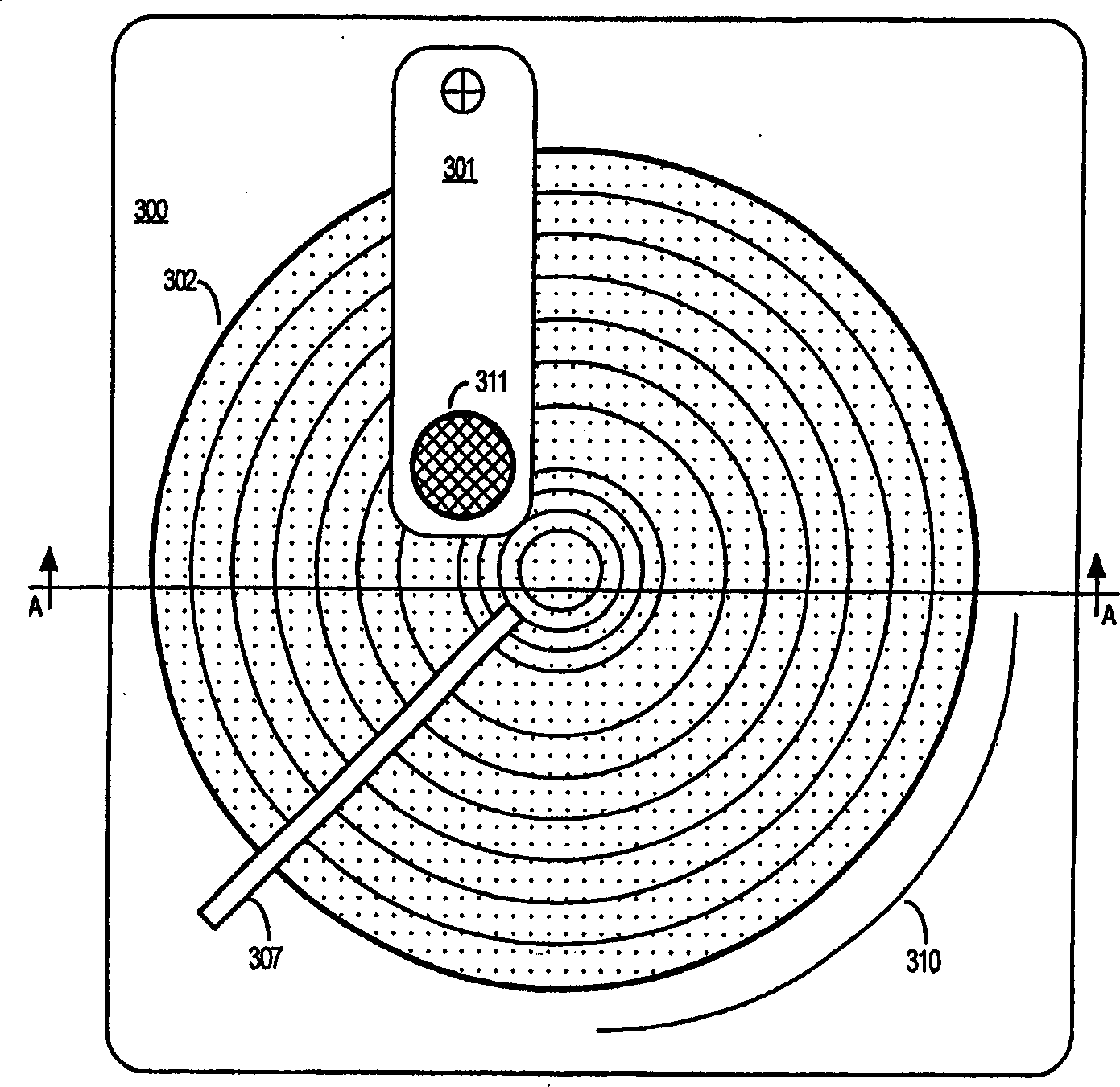
[0025] Reference will now be made in detail to the preferred embodiments of the present invention, a method and system for in situ optimization of semiconductor wafers in a chemical mechanical polishing process, examples of which are illustrated in the accompanying drawings. While the invention has been described in conjunction with the preferred embodiments, it is to be understood that the invention is not limited to those embodiments. On the contrary, the invention is intended to cover alternatives, modifications and equivalents included in the spirit and scope of the invention as defined in the appended claims. Moreover, in the following detailed description of the invention, numerous specific details are set forth in order to provide a thorough understanding of the invention. However, it will be apparent to one skilled in the art that the present invention may be practiced without these specific details. In other instances, well-known methods, procedures, components, and ...
PUM
 Abstract
Description
Claims
Application Information