
Connection structure for display module and printed base plate and semiconductor device, display module and electronic member

A technology for printed substrates and display modules, applied in the directions of printed circuit components, structural connection of printed circuits, printed circuits, etc., can solve problems such as unfavorable thin installation, and achieve stable conduction and reliable contact

Inactive Publication Date: 2002-03-20
SHARP KK
View PDF1 Cites 13 Cited by
  • Summary
  • Abstract
  • Description
  • Claims
  • Application Information

AI Technical Summary

Problems solved by technology

Therefore, it is disadvantageous in terms of thin mounting

Method used


Image

  • Connection structure for display module and printed base plate and semiconductor device, display module and electronic member
  • Connection structure for display module and printed base plate and semiconductor device, display module and electronic member
  • Connection structure for display module and printed base plate and semiconductor device, display module and electronic member

Examples


Embodiment 1

[0053] Hereinafter, an embodiment of a connection structure between a display module and a printed circuit board, a semiconductor device, a display module, and electronic components of the present invention will be described.

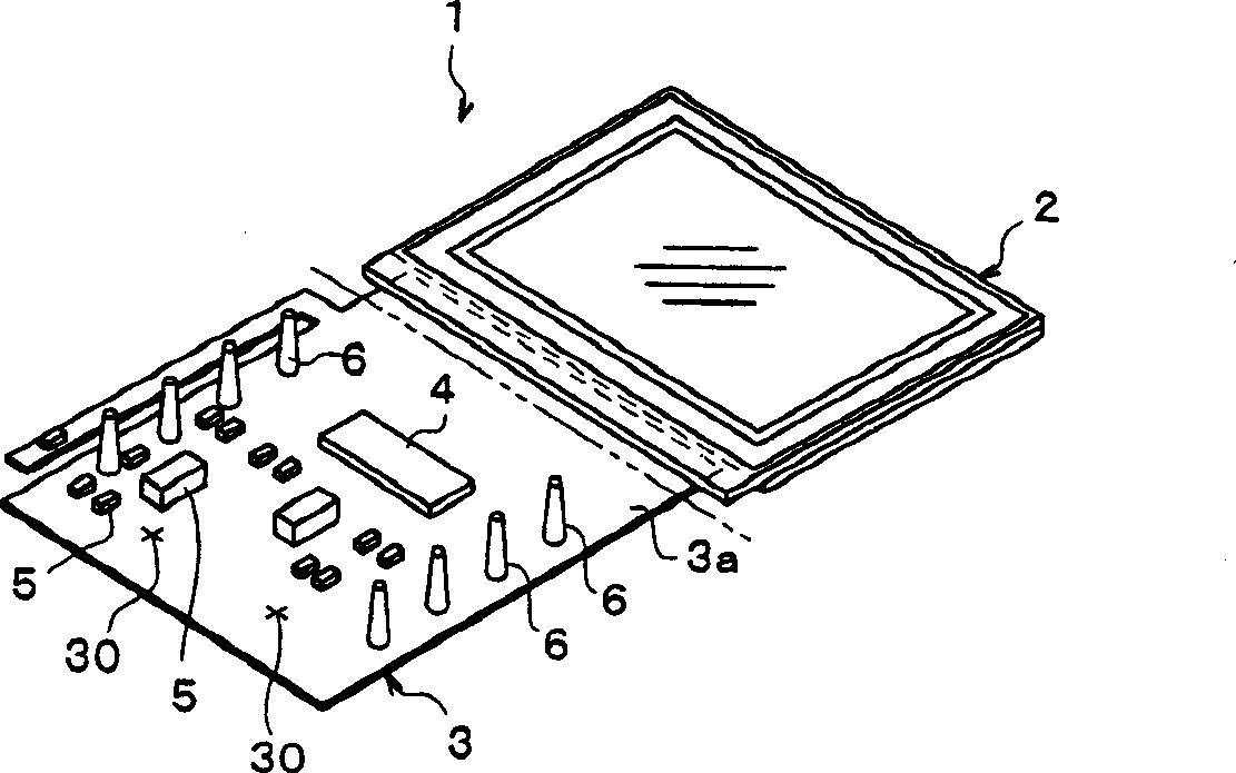
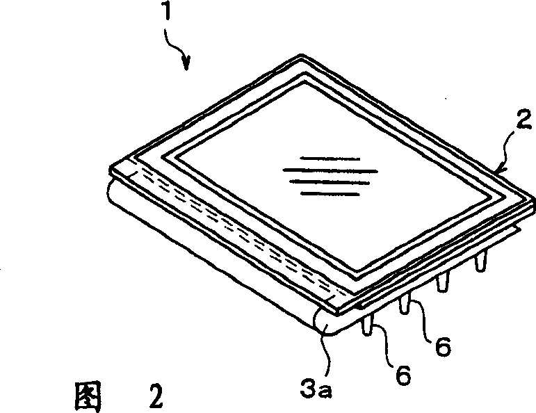
[0054] exist figure 1 2 shows a liquid crystal module (display module) 1 in which a liquid crystal panel (display panel) 2 and a COF 3 serving as a liquid crystal driver (semiconductor device) are connected. A semiconductor element 4 constituting a liquid crystal driver IC and a plurality of mounting components 5 .

[0055] Furthermore, in this COF 3 , conventionally, planar electrodes are formed on the external connection terminals. In addition, the so-called external connection terminals are terminals for connecting the wiring formed on the flexible wiring board 3a and the electrodes of the printed board described later.

[0056] On the other hand, in this embodiment, pin-shaped pin electrodes (protrusion-shaped electrodes) 6 . . . formed of a cond...

Embodiment 2

[0075] Below, use Figure 6 and Figure 7 , illustrating another embodiment of the connection structure between the display module and the printed substrate, the semiconductor device, the display module, and the electronic component of the present invention. In addition, for the convenience of description, the components having the same functions as those shown in the drawings of the first embodiment are given the same reference numerals, and their descriptions are omitted.

[0076] Figure 6 A liquid crystal module (display module) 20 in this embodiment is shown in . The liquid crystal module 20 has COF21 instead of COF3 in the structure of the liquid crystal module 1. In addition, COF21 has bump electrode 22... instead of pin electrode 6... in the structure of COF3.

[0077] That is, the semiconductor element 4 and the plurality of mounting parts 5 constituting the liquid crystal driver IC are mounted on the flexible wiring substrate 3a as the base of the COF 21. In this r...

Embodiment 3

[0083] Below, use Figure 8 , to describe another embodiment of the connection structure between the display module and the printed substrate, the semiconductor device, the display module, and the electronic components of the present invention. In addition, for the convenience of description, the components having the same functions as those shown in the drawings of the first embodiment are given the same reference numerals, and their descriptions are omitted.

[0084] Figure 8 A liquid crystal module (display module) 25 in this embodiment is shown in . The liquid crystal module 25 has COF26 instead of COF3 in the structure of the liquid crystal module 1. Moreover, COF26 has the spring electrode 27 instead of the pin electrode 6... in the structure of COF3.

[0085] That is, the semiconductor element 4 and the plurality of mounting parts 5 constituting the liquid crystal driver IC are mounted on the flexible wiring substrate 3a as the base of the COF 26. In this regard, th...


PUM

PropertyMeasurementUnit
thicknessaaaaaaaaaa

Abstract

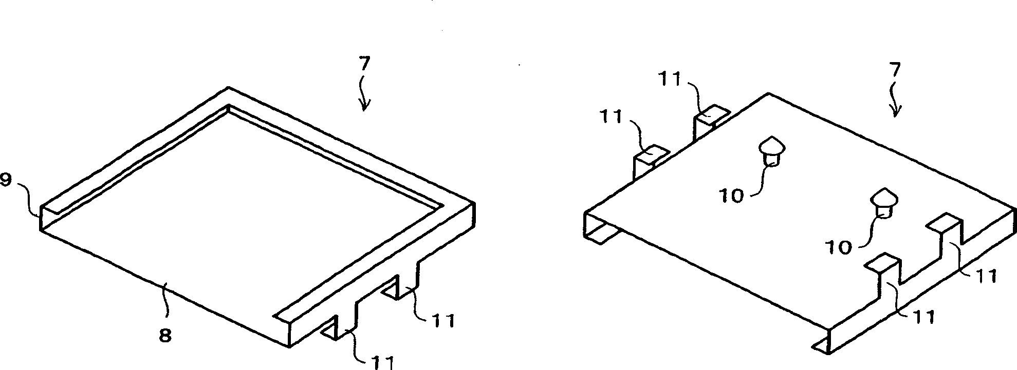
A connection structure for connecting a display module and a printed substrate is provided, which is appropriate for use in mass production of electronic devices such as a cellular phone in which, while a thin mounting is desired, many components have to be mounted on the printed substrate and the display module is required to be mounted in predetermined space on the printed substrate. The liquid crystal module is provided with a pin electrode on an external connection terminal of its COF, and fixed to a housing in a folded state with respective rear surfaces of the COF and a liquid crystal panel facing each other. A holding member for engaging the printed substrate and holding the printed substrate is formed on the housing. When the holding member engages the printed substrate, the liquid crystal module is fixed to the printed substrate, and at the same time, the pin electrode of the COF and a through hole electrode of the printed substrate are electrically connected.

Description

technical field [0001] The present invention relates to a connection structure between a display module and a printed substrate for connecting a display module formed by bonding a semiconductor element and connecting a semiconductor device mounted on a flexible wiring substrate to a display panel to a printed substrate, and a semiconductor used in the connection structure A device, a display module, and an electronic component formed by connecting the display module to a printed substrate using the connection structure, and more specifically, relates to an electronic device suitable for use in an electronic device requiring high-density wiring such as a mobile phone or a portable alarm clock. A connection structure between a display module and a printed circuit board, a semiconductor device, a display module, and an electronic component. Background technique [0002] Conventionally, in electronic devices such as mobile phones and portable alarm clocks, semiconductor devices ...

Claims


Application Information

Patent Timeline
Patent Type & Authority Applications(China)
IPC IPC(8): G02F1/1333G02F1/13G02F1/1345G09F9/00H01R12/62H04M1/02H05K1/14H05K1/18H05K3/30H05K3/36H05K7/14
CPCH05K2201/10136H05K3/365H05K1/147H04M1/0266H05K3/301H05K1/189H05K1/141G02F1/13452
Inventor 千川保宪佐藤邦浩友国博章
Owner SHARP KK
Learn More