Liquid crystal display device

A liquid crystal display and device technology, applied in the field of so-called partially transmissive active matrix liquid crystal display devices, can solve problems such as insufficient efficiency

Inactive Publication Date: 2002-06-19
JAPAN DISPLAY INC
View PDF0 Cites 7 Cited by
  • Summary
  • Abstract
  • Description
  • Claims
  • Application Information

AI Technical Summary

Problems solved by technology

[0013] However, there is a drawback in making a reflective electrode in this way, that is, using the light from the backlight unit as the required transmitted light to re-reflect it will result in little efficiency since Mo is less reflective than aluminum.

Method used


Image

  • Liquid crystal display device
  • Liquid crystal display device
  • Liquid crystal display device

Examples


Embodiment 1

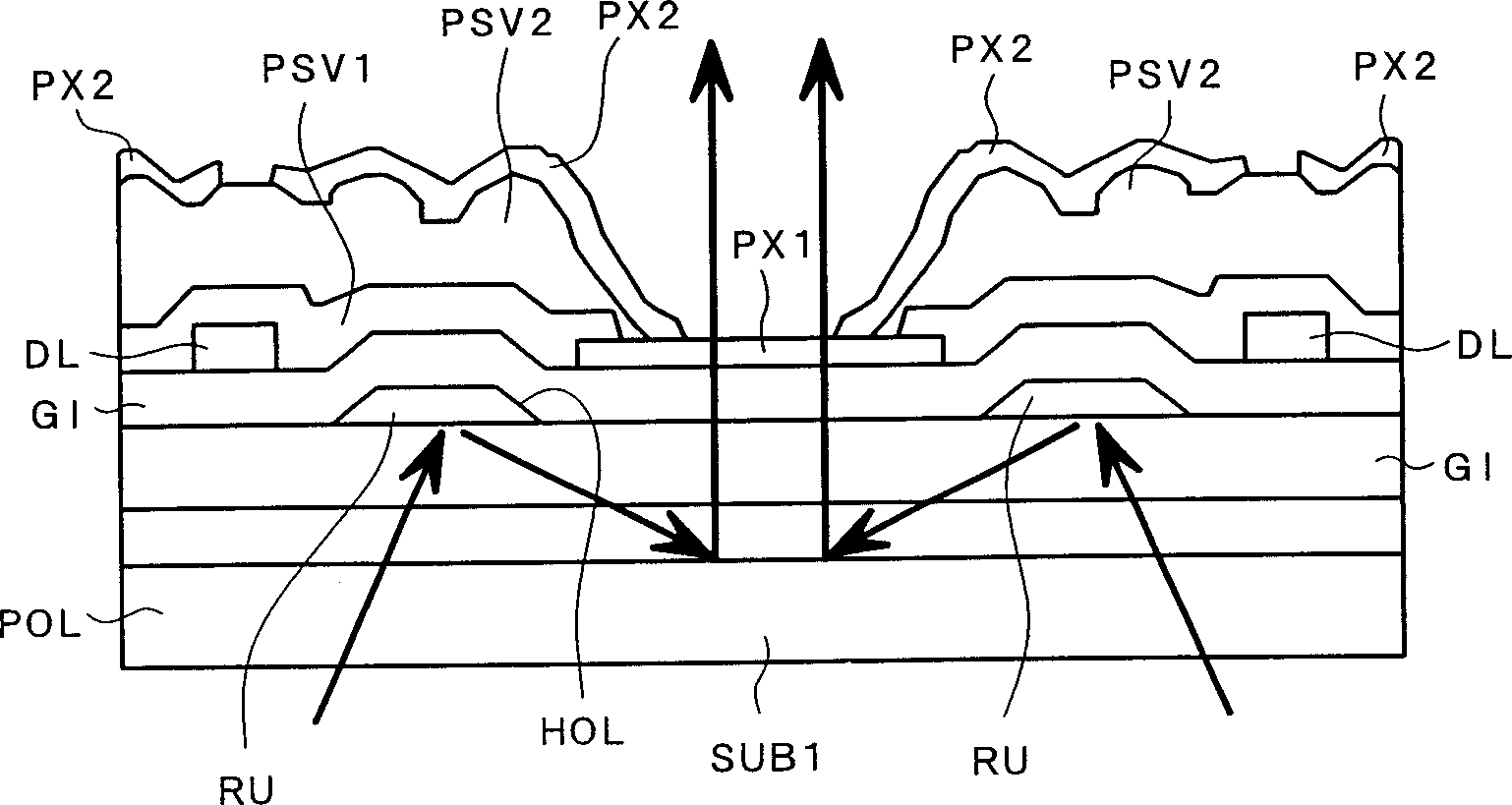
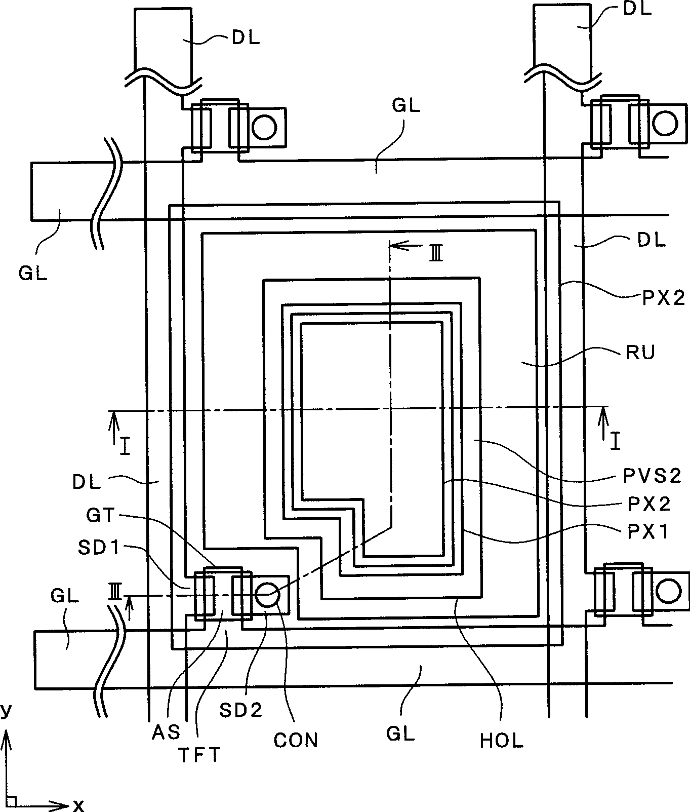
[0034] figure 2 It is a plan view of a pixel structure of a liquid crystal display device according to an embodiment of the present invention. also, figure 1 shows along the figure 2 Pixel cross-sectional view of midline I-I; image 3 shows along the figure 2 Pixel cross-sectional view of midline III-III.

[0035] figure 2 shows a plan view of a single pixel among the pixels arranged in a matrix, and the other pixels located around or above and below the pixel are similar in structure to the pixel shown.

[0036] exist figure 2 In this method, gate signal lines GL are first arranged on the surface of a transparent substrate SUB1 so that these lines extend along the "x" direction in the figure and are parallel to each other in the "y" direction.

[0037] As will be explained later, a region surrounded by these gate signal lines and drain signal lines extending along the “y” direction in the figure and parallel to each other in the “x” direction is defined as a pixel...

Embodiment 2

[0070] Figure 4 is a plan view of a pixel structure of a liquid crystal display device according to another embodiment of the present invention, corresponding to figure 2 . also, Figure 5 for along Figure 4 The midline V-V looks at the cross-sectional view of the pixel, while Figure 6 for along Figure 4 Cross-sectional view of midline VI-VI.

[0071] and figure 2 The difference in the structure shown in is that the light reuse film RU is integrated with the light reuse film RU in the adjacent pixel area along the x direction in the figure (ie along the extension direction of the gate signal line GL).

[0072] More specifically, the light reuse film RU extends to the bottom portion of the drain signal line DL.

[0073] As mentioned above, the drain signal line DL is made of the same material as the drain SD1 and source SD2 of the thin-film transistor TFT, and they are all made of continuously pressed or "multi-layered" high-melting-point metals (Mo, Ti, Ta, Cr) a...

Embodiment 3

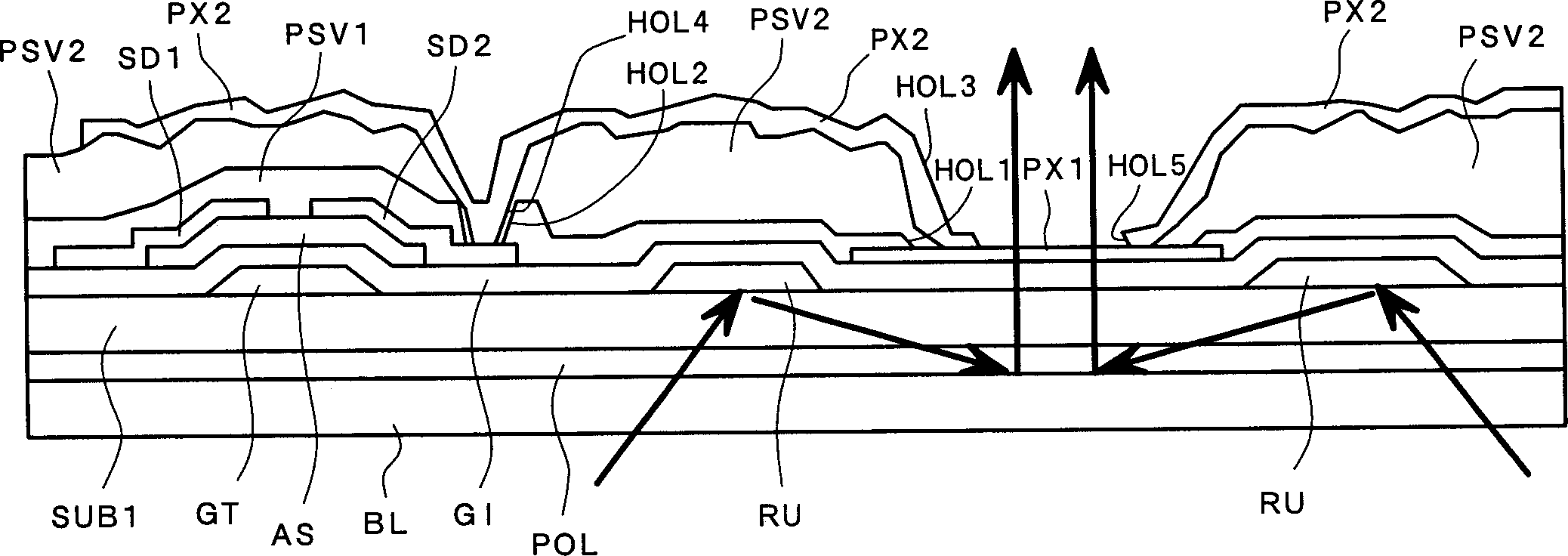
[0083] Figure 7 It is a plan view of a pixel structure of a liquid crystal display device according to yet another embodiment of the present invention, corresponding to Figure 5 . in addition, Figure 8 for along Figure 7 Cross-sectional view of midline VIII-VIII.

[0084] Figure 7 The embodiment shown in the structure of embodiment 2 has been further improved. The main difference from Embodiment 2 is that the light reuse film RU is physically divided into fragments, and these fragments form many mutually separated light reuse films RU1 on the same layer (the upper surface of the electrically insulating film GI).

[0085]The reason for adopting such a split structure of the light reuse film RU is as follows: When one drain signal line DL is electrically short-circuited with the light reuse film RU below it for some reason, The capacitive coupling between the RU and the pixel electrode PX causes a potential change or deviation on the pixel electrode PX, and an operati...


PUM


Abstract

To improve optical transmission efficiency without reducing optical reflection efficiency. While rays of light coming from a backlight are irradiated from the side of one substrate of respective substrates disposed to oppose each other with a layer of liquid crystal material interposed therebetween, a certain region on a liquid crystal side surface of the one substrate which is surrounded by neighboring gate signal lines being disposed adjacent to each other and drain signal lines being disposed adjacent to each other is adapted for use as a pixel region, in which a pixel electrode is formed for receiving an image signal as supplied from one drain signal line via a thin-film transistor rendered operative by supplement of a scan signal from one gate signal line, wherein this pixel electrode is generally made up from a conductive reflection film and a transparent conductive film that are electrically connected together with a light reclamation or ''reuse'' film being formed beneath the conductive reflection film through the conductive reflection film and a dielectric film, this light reuse film being electrically insulated from either the gate signal lines or the drain signal lines.

Description

technical field [0001] The present invention relates to liquid crystal display devices, and in particular to so-called partially transmissive active matrix liquid crystal display devices for transmissive and reflective displays. Background technique [0002] In a general active matrix liquid crystal display, the gate signal (gate signal) line extending along the "x" direction and parallel to the "y" direction and the drain signal (drain signal) extending along the "y" direction and parallel to the "x" direction ) lines are formed on the liquid crystal side surfaces of the substrates facing each other with a layer of liquid crystal material interposed therebetween, wherein the area delimited by these signal lines is used as a picture element or "pixel" area. [0003] In such a pixel area, there is a thin film transistor and a pixel electrode, wherein the thin film transistor is selected by a scan signal provided by a gate signal arranged along one side thereof, and the pixel ...

Claims


Application Information

Patent Timeline
Patent Type & Authority Applications(China)
IPC IPC(8): G02F1/1335G02F1/13357G02F1/1343G09F9/30
CPCG02F1/133555G02F1/1335
Inventor 小野记久雄平方纯一落合孝洋桶隆太郎
Owner JAPAN DISPLAY INC
Why Eureka
Try Eureka