

Semiconductor device and method of manufacturing the same
A device manufacturing method and semiconductor technology, applied in semiconductor/solid-state device manufacturing, semiconductor devices, electrical solid-state devices, etc., can solve the problems of NAND-type EEPROM electrical reliability reduction and other issues
- Summary
- Abstract
- Description
- Claims
- Application Information
AI Technical Summary
Problems solved by technology
Method used
Image

Examples
no. 1 Embodiment
[0050] [Semiconductor device structure with non-volatile memory circuit]
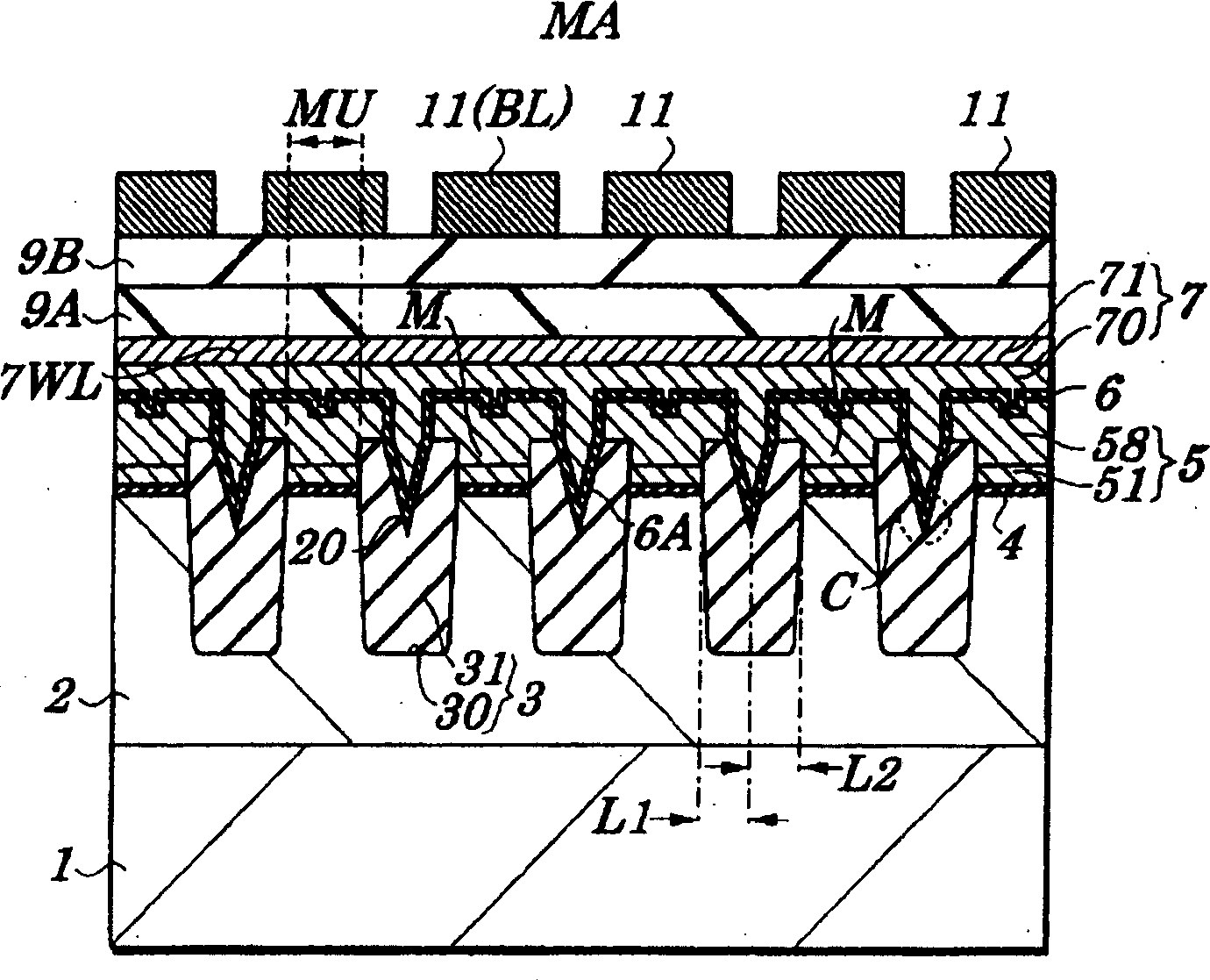
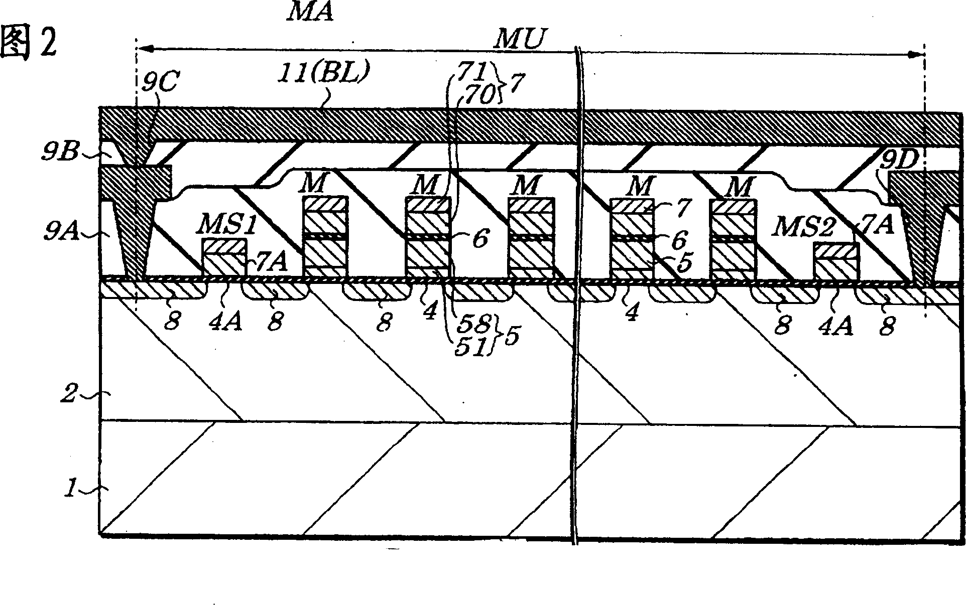
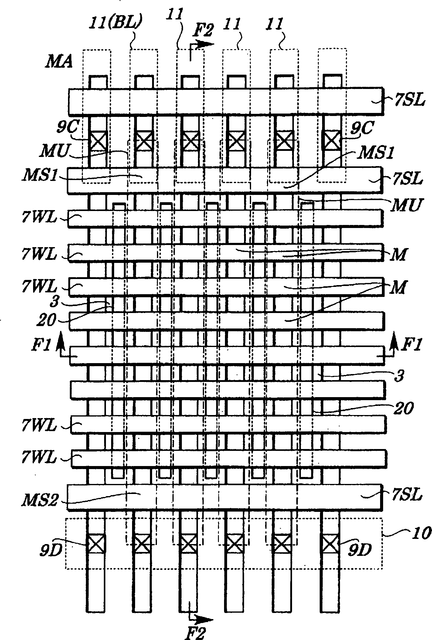
[0051] The first embodiment of the present invention is to describe a semiconductor device equipped with a NAND-type EEPROM. Here, the term “semiconductor device” is used in the sense that it includes at least a semiconductor memory with only NAND-type EEPROM function, and a semiconductor device that includes logic circuits and other circuits on the same substrate in addition to NAND-type EEPROM.
[0052] Such as Figure 1 to Figure 3 As shown, the NAND-type EEPROM according to the first embodiment of the present invention includes memory cells M arranged in rows and columns on a semiconductor substrate 1 (or well region 2), the memory cells M having a floating electrode (floating gate electrode) 5 memory cells MA; between the memory cells M along the gate width direction (the direction in which the word line extends), there is a first trench 30 provided in the depth direction from the surface of the semico...
no. 2 Embodiment
[0113] The second embodiment of the present invention is to describe an example of replacing the cross-sectional shape of the second groove 20 in a semiconductor device provided with the NAND-type nonvolatile memory circuit of the first embodiment of the present invention.
[0114] A semiconductor device having a NAND-type nonvolatile memory circuit according to the second embodiment of the present invention, such as Picture 12 As shown, the isolation filling material 31 of the element isolation region 3 is provided with a second groove 21 having a U-shaped cross-sectional shape. That is, as with the second groove 20 of the first embodiment of the present invention, the groove width of the second groove 21 facing the surface portion in the grid width direction, and the groove width forming the depth portion is small. Therefore, the separation distances L1 and L2 between the sidewall of the second groove 21, particularly the bottom of the well region 2 and the well region 2 can be...
no. 3 Embodiment
[0119] The third embodiment of the present invention is to describe an example of replacing the cross-sectional shape of the second groove 20 in a semiconductor device equipped with a NAND-type nonvolatile memory circuit of the first embodiment of the present invention.
[0120] A semiconductor device equipped with a NAND-type nonvolatile memory circuit according to the third embodiment of the present invention, such as Figure 13 As shown, the isolation filling material 31 of the element isolation region 3 is provided with a second groove 22 having an inverted mesa-shaped cross-sectional shape. That is, as with the second groove 20 of the first embodiment of the present invention, the groove width of the second groove 22 in the grid width direction to the surface portion and the groove width forming the depth portion is small. Therefore, the separation distances L1 and L2 between the sidewalls of the second groove 22, particularly the bottom of the well region 2 and the well regi...
PUM
 Abstract
Description
Claims
Application Information