
Semiconductor package with electrical connection structure and manufacturing method thereof

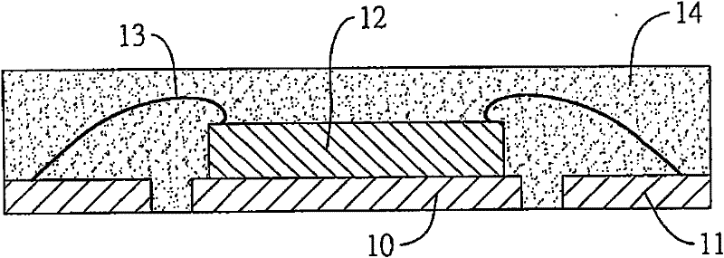
An electrical connection and semiconductor technology, applied in the field of packaging structure and its manufacturing method, can solve the problems of increased manufacturing cost, different thermal expansion coefficients, long gold wires 23, etc., to reduce the length of the bonding wire, improve the adhesion strength, and avoid scratching. effect of injury

Active Publication Date: 2011-07-20
SILICONWARE PRECISION IND CO LTD
View PDF5 Cites 3 Cited by
  • Summary
  • Abstract
  • Description
  • Claims
  • Application Information

AI Technical Summary

Problems solved by technology

[0010] Although the anti-oxidation layer 25 covers part of the area of ​​each of the bump pads 21, the anti-oxidation layer 25 is formed on the bottom of the encapsulant 24, and the thermal expansion between the anti-oxidation layer 25 and the encapsulant 24 The coefficients (CET) are not the same, resulting in the phenomenon of delamination (delamination) between the anti-oxidation layer 25 and the encapsulant 24.
like Figure 2E As shown, if there is delamination between the anti-oxidation layer 25 and the encapsulant 24, it is easy to penetrate due to water vapor, which will cause leakage of the protruding pad 21 due to water vapor, and then lead to the electrical operation. Is not functioning properly, thus affecting the overall electrical function
Furthermore, if Figure 2C As shown, the protruding pads 21 are flush with the surface of the encapsulant 24, causing the protruding pads 21 to be easily scratched during the manufacturing process; in addition, two adjacent protruding pads 21 may also be damaged during the reflow process or Due to the thermal cycle effect of the actual use of the product, the solder ball 26 leaks into the interface between the anti-oxidation layer 25 and the encapsulant 24, causing leakage or even a short circuit problem.
[0011] In addition, the chip 22 is electrically connected to the bump pad 21 with gold wires 23. If the bump pad 21 is far from the chip 22, a longer gold wire 23 needs to be used, which increases the manufacturing cost.
[0012] Therefore, in view of the above-mentioned problems, how to avoid current leakage caused by delamination and moisture infiltration caused by different thermal expansion coefficients of existing semiconductor packages, avoid solder pad scratches, avoid solder ball bridging, and avoid electrical leakage caused by solder material leakage. Sexual short circuit and avoiding the high cost caused by too long gold wire have become urgent problems to be solved at present.

Method used


Image

  • Semiconductor package with electrical connection structure and manufacturing method thereof
  • Semiconductor package with electrical connection structure and manufacturing method thereof
  • Semiconductor package with electrical connection structure and manufacturing method thereof

Examples


Embodiment Construction

[0056] Embodiments of the present invention are described below through specific examples, and those skilled in the art can easily understand other advantages and effects of the present invention from the content disclosed in this specification.

[0057] It should also be noted that the "top surface" and "bottom surface" described in this specification are not absolute spatial concepts, but change with the spatial relationship of the constituent elements. In the case of semiconductor packages, the "top surface" is the "bottom surface" and the "bottom surface" is the "top surface". Therefore, the use of the term "top surface" and "bottom surface" is to illustrate the connection relationship between the constituent elements in the semiconductor package provided by the present invention, so that the semiconductor package provided by the present invention is within the equivalent range There are reasonable changes and substitutions, but not intended to limit the scope of the prese...


PUM


Abstract

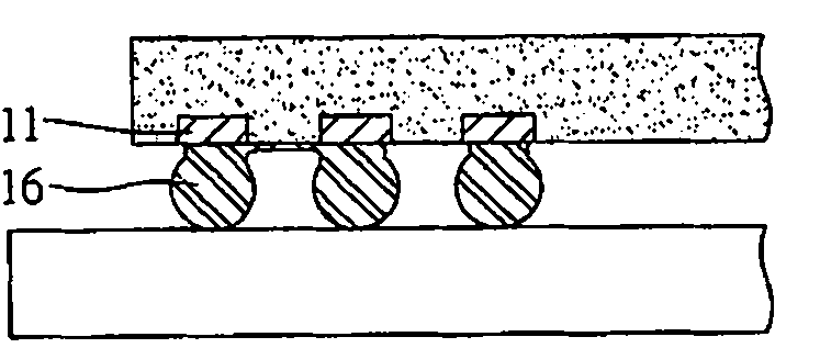
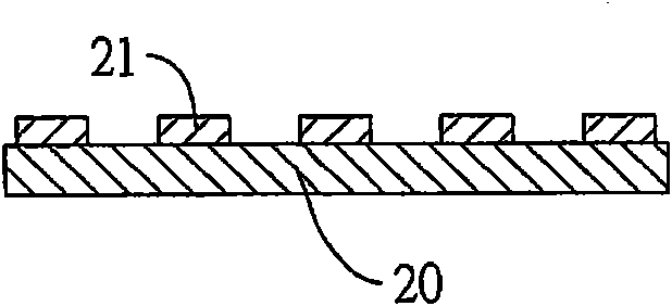
The invention provides a semiconductor package with an electrical connection structure and a manufacturing method thereof, and the semiconductor package comprises a conducting wire layer, a chip, a welding wire, a packaging colloid, an anti-welding layer and welding balls, wherein the conducting wire layer comprises a chip carrier and a plurality of conducting wires annularly arranged on the periphery of the chip carrier; the packaging colloid comprise a plurality of recesses which are used for embedding the chip carrier and the conducting wires, in the depth of greater than the thickness of the chip carrier and the conducting wires and further exposed on the surface of the conducting wires and the chip carrier; the anti-welding layer is formed in the recesses of the packaging colloid, and the anti-welding layer comprises a plurality of open holes of the anti-welding layer for exposing all conducting wire terminals and part of the chip carrier; and the welding balls are formed in all the open holes of the anti-welding layer to electrically connect with the corresponding conducting wire terminals. Therefore, the adhesion strength of the anti-welding layer is improved by mutual embedding and clamping between the anti-welding layer and the packaging colloid, a path for enabling wet gas to infiltrate into the package is prolonged, and the product reliability is enhanced.

Description

technical field [0001] The present invention relates to a packaging structure and a manufacturing method thereof, in particular to a semiconductor package (Quad Flat Non Leaded Package, QFN) with an electrical connection structure and a manufacturing method thereof. Background technique [0002] A traditional chip uses a lead frame (Lead Frame) as a chip carrier to form a semiconductor package, and the lead frame mainly includes a chip seat and a plurality of guide pins formed around the chip seat. After the chip is electrically connected to the lead pins by bonding wires, packaging resin is used to coat the chip, the chip holder, the bonding wires and the inner sections of the lead pins to form the semiconductor package with a lead frame. [0003] As far as the development of integrated circuit technology is concerned, the semiconductor manufacturing process is constantly evolving towards a more highly integrated process, and a high-density assembly structure is the goal pu...

Claims


Application Information

Patent Timeline
Patent Type & Authority Applications(China)
IPC IPC(8): H01L23/49H01L23/31H01L23/488H01L21/50H01L21/56
CPCH01L2224/45144H01L2224/48247H01L2924/00
Inventor 林邦群李春源汤富地黄建屏柯俊吉
Owner SILICONWARE PRECISION IND CO LTD
Learn More