Eureka AIR delivers breakthrough ideas for toughest innovation challenges, trusted by R&D personnel around the world.

Film thickness monitoring method and substrate temperature detecting method

A technology for temperature measurement and film thickness, which is used in semiconductor/solid-state device testing/measurement, gaseous chemical plating, coating, etc., which can solve the problems of taking out the substrate, unable to know the film thickness on site, impossible, etc.

Inactive Publication Date: 2002-11-06
KK TOSHIBA
View PDF0 Cites 4 Cited by
  • Summary
  • Abstract
  • Description
  • Claims
  • Application Information

AI Technical Summary

Problems solved by technology

[0007] However, in the above-mentioned first prior art, the film thickness cannot be known on-site during film formation, but the film thickness can only be confirmed after film formation.
For this reason, even if a film thickness different from the target film thickness is formed for some reason during film formation, the formation of a different film thickness cannot be avoided in advance.
[0008] In addition, in the above-mentioned second prior art, in the batch diffusion furnace generally used for the formation of the gate oxide film, since dummy substrates are provided above and below the substrate for manufacturing semiconductor devices, there is no actual Possibility of extracting radiated light from the substrate through glass fibers

Method used


Image

  • Film thickness monitoring method and substrate temperature detecting method
  • Film thickness monitoring method and substrate temperature detecting method
  • Film thickness monitoring method and substrate temperature detecting method

Examples


Embodiment Construction

[0019] Hereinafter, embodiments of the present invention will be described with reference to the drawings. In the following description, common reference signs are used in common parts of all figures.

[0020] First implementation form

[0021] Next, the film thickness monitoring method in the CVD apparatus according to the first embodiment of the present invention will be described.

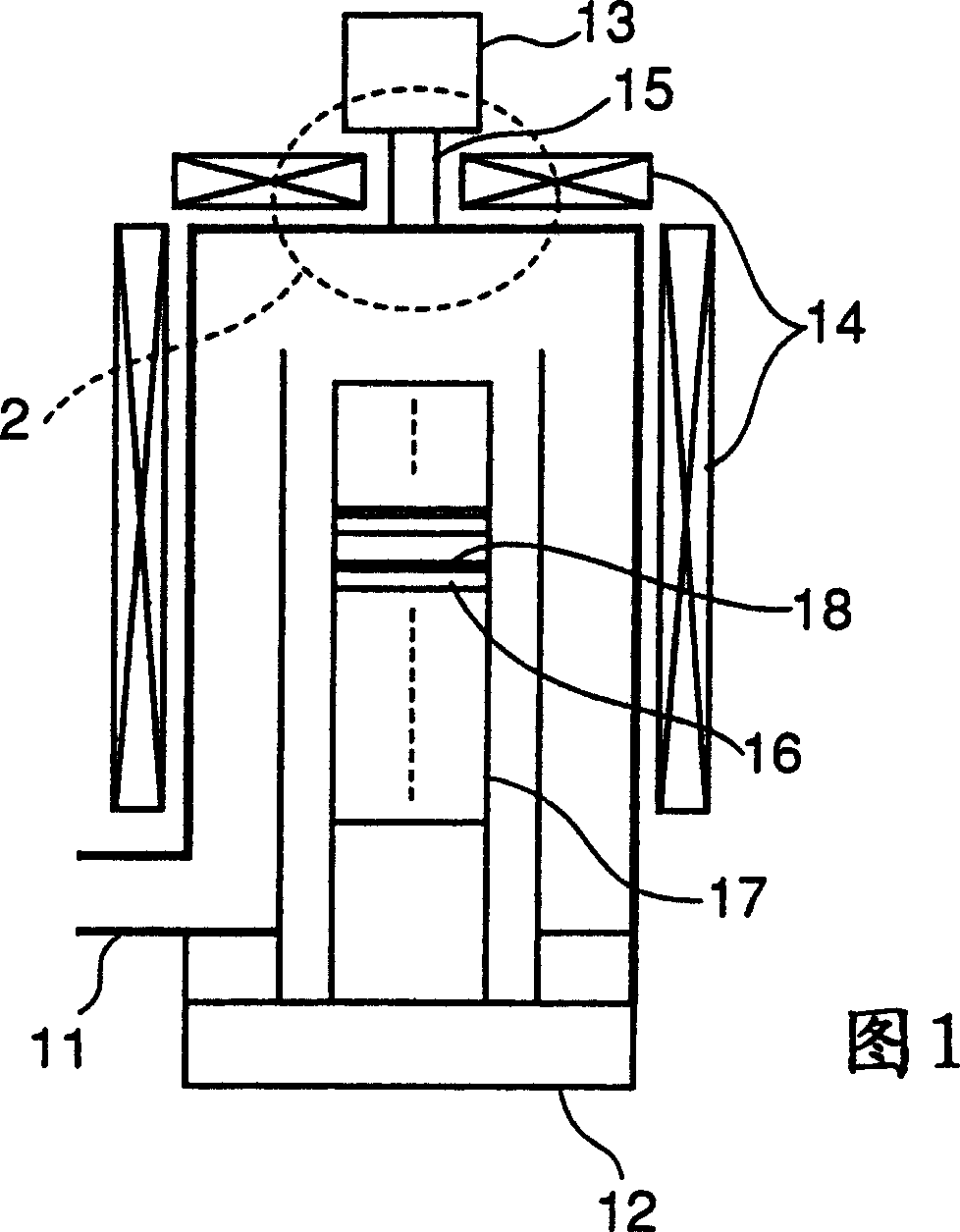
[0022] FIG. 1 is a diagram showing the structure of a CVD apparatus used in the film thickness monitoring method of the first embodiment. The CVD apparatus shown in the figure is a vertical LPCVD apparatus.

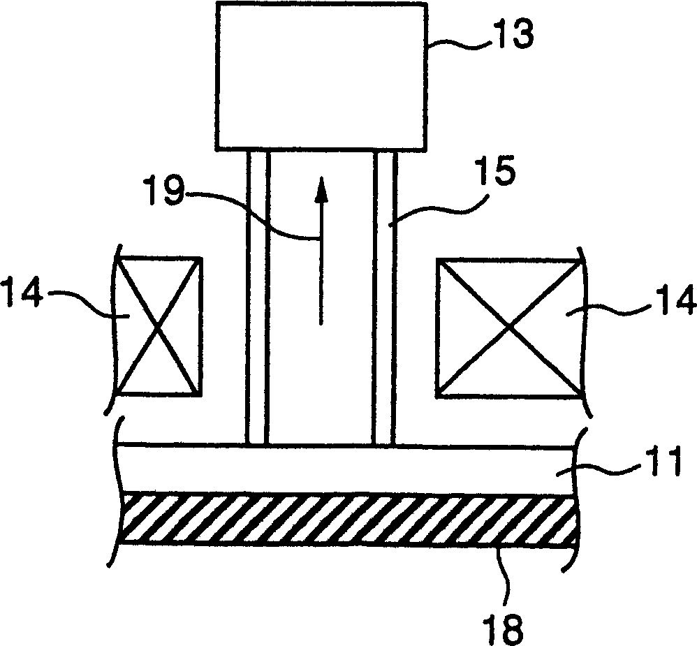
[0023] As shown in FIG. 1, the vertical LPCVD apparatus includes a reaction furnace having a quartz tube 11, a sealing cover 12, a radiation thermometer (pyrometer) 13, and a heater 14. A radiation thermometer 13 is installed on the quartz tube 11 in the upper part of the reaction furnace through the introduction tube 15. A heater 14 is provided on the side and upper surface of the quartz tube ...


PUM

PropertyMeasurementUnit
wavelengthaaaaaaaaaa

Abstract

The film thickness monitoring method of the present invention viewed from one side is configured as follows. When a thin film is formed on a substrate in the reaction furnace using a CVD (Chemical Vapor Deposition) apparatus having a reaction furnace, the radiation light from the reaction furnace is measured outside the reaction furnace to obtain the emissivity of the radiation light. The relationship between the change and the film thickness change of the thin film formed on the above-mentioned substrate. When a thin film is formed on a substrate using the CVD apparatus after obtaining the relationship between the change in emissivity and the change in film thickness, the change in emissivity of the radiated light is measured. The film thickness of the thin film formed on the substrate in the reaction furnace is estimated from the measured change in the emissivity of the radiated light based on the obtained relationship between the emissivity change and the film thickness change.

Description

Technical field [0001] The invention relates to a film thickness monitoring method for monitoring the film thickness on a substrate in a reaction furnace of a CVD device on site, and a film thickness control adopting a method for measuring the substrate temperature in a diffusion furnace. Background technique [0002] Next, the conventional film thickness monitoring method (first prior art) for monitoring the film thickness of the film formed in the furnace of the CVD apparatus on site will be described. [0003] In the past, in the manufacture of semiconductor devices, a CVD (Chemical Water Vapor Deposition) device was used to form a thin film on a semiconductor substrate (sheet). [0004] However, a high-temperature thermal process is required in the CVD apparatus, and when a thin film is formed by the CVD apparatus, there is no method for monitoring the film thickness on site. Therefore, under the current situation, the film thickness is generally measured by the following met...

Claims


Application Information

Patent Timeline
Patent Type & Authority Applications(China)
IPC IPC(8): C23C16/52H01L21/205H01L21/22H01L21/28H01L21/285H01L21/302H01L21/3065H01L21/66
CPCC23C16/52H01L22/00
Inventor 赤堀浩史佐俣秀一
Owner KK TOSHIBA
Why Eureka
Eureka Blog
Learn More