
NXN light exchanging structure in full photo exchanging nodal point

An all-optical switching and optical switching technology, applied in wavelength division multiplexing systems, selection devices, electrical components, etc., can solve the problems of system complexity, device cost increase, and the number of passive devices, etc., to achieve the goal of reducing crosstalk Effect

Inactive Publication Date: 2003-01-22
HUAZHONG UNIV OF SCI & TECH
View PDF0 Cites 27 Cited by
  • Summary
  • Abstract
  • Description
  • Claims
  • Application Information

AI Technical Summary

Problems solved by technology

[0016] There are many ways to eliminate crosstalk. At present, the methods of eliminating crosstalk at home and abroad mainly include: (1) Through the design of the network node topology, the amount of crosstalk is converted from low-order to high-order, thereby eliminating the impact of crosstalk on the transmission system to a certain extent. However, it will inevitably lead to the complexity of network nodes and the increase in the number of passive devices, and the cost of a single network node will also increase.
(2) Reduce crosstalk by focusing on improving the performance of passive devices in network nodes, which will inevitably increase the cost of devices, and at the same time, crosstalk cannot be well eliminated when the scale of switching nodes is large
(3) By scrambling the transmitted optical signal and its phase, this will lead to system complexity and is only suitable for local networks
Thereby above-mentioned method all can not thoroughly eliminate the crosstalk in the DWDM optical communication system, and its method for eliminating crosstalk mostly considers from one side: on the one hand they only consider the topological structure of the network; device performance to reduce crosstalk
However, none of them are integrated with the DWDM system, so the degree of reduction of crosstalk is also limited.

Method used


Image

  • NXN light exchanging structure in full photo exchanging nodal point
  • NXN light exchanging structure in full photo exchanging nodal point
  • NXN light exchanging structure in full photo exchanging nodal point

Examples


Embodiment Construction

[0031] Specific implementation

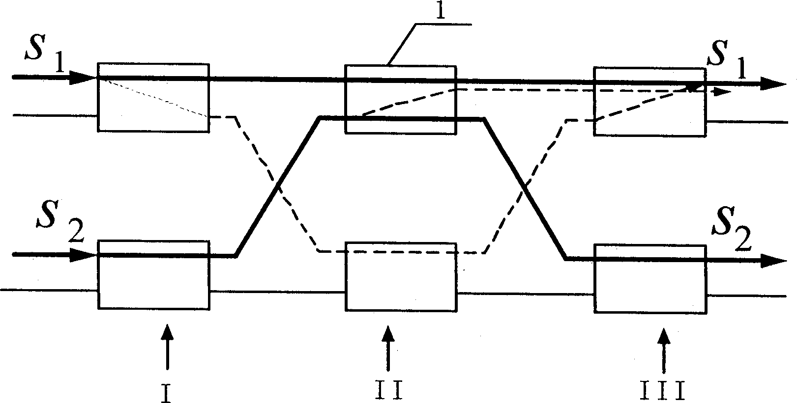
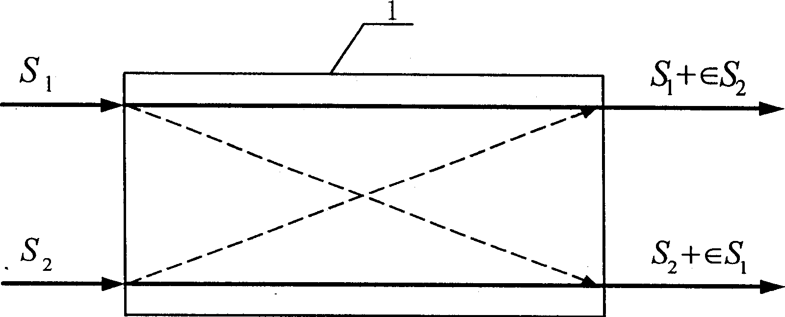
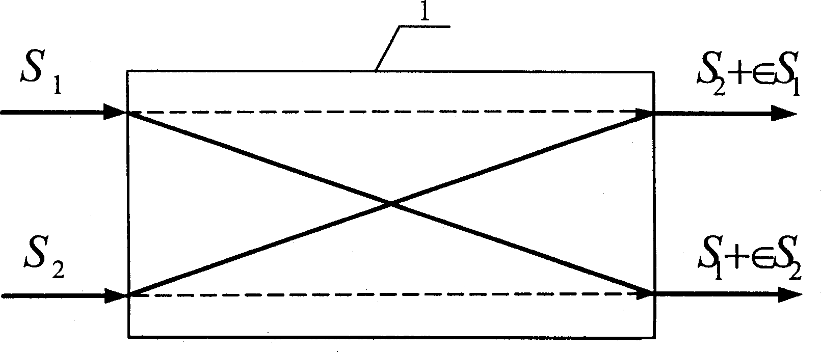
[0032] The structure of the present invention is as Figure 5 As shown, the extended Bense optical switching structure called reconstruction can greatly reduce crosstalk. For an N×N extended Bense optical switching structure, such as Figure 6 As shown in the recursive decomposition, 3 in the figure represents the optical switch 1 Optical switching structure, so Figure 5 with Figure 4 The only difference is that the semiconductor optical amplifier "on / off" gate 2 is added between the recursive decomposition level II and level III to form the V level. In this way, adding the semiconductor optical amplifier "on / off" gate 2 only makes an equivalent change to the routing, and therefore not only does not change some of the excellent properties of the extended Bense optical switching structure, such as: generalized non-blocking, hardware optimality, etc., at the same time It also has a good effect on reducing crosstalk.

[0033] The present invention ...


PUM


Abstract

This invention relates to a NxN optical exchange structure for all-optical exchange nodal points composed of 2n stages, in which n=log2N characterized by a "on / off" gate of a semiconductor amplifier between nth stage and n+1th stage forming 2n+1th stage; or different numbers of semiconcutor optical mplifier "on / off" gates can be designed in any second stage optical switches according to specific need. This invention uses restructured enlarge Bense optical exchange structure to limit the rrosstalk. A semiconductor optical amplifier "on / off" gate (SOA gate) is added to a NxN enlarge Bense optical exchange structure with equivalent variance to the route. The invention reserves good performances of the enlarged Bense optical exchange structure; generalized unblockness, optimality of the hardware, and reduced crosstalk.

Description

Technical field [0001] The invention belongs to the technical field of optical communication devices, and specifically relates to an N×N optical switching structure used in an all-optical switching node. It is especially suitable for DMDW systems and can solve the crosstalk in the N×N all-optical switching node in the system. problem. Background technique [0002] With the continuous development and wide application of IP technology, the capacity and colorful business volume of optical communications are showing an exponential growth trend. Optical networks based on Dense Wavelength Division Multiplexing (DWDM) technology have been recognized as the most effective way to alleviate the increasing communication capacity. The establishment of optical networks and the exchange of information between channels are bound to introduce all-optical switching nodes into the network topology. The all-optical switching node is generally composed of a wavelength division multiplexer (MUX), an ...

Claims


Application Information

Patent Timeline
Patent Type & Authority Applications(China)
IPC IPC(8): H04J14/02H04Q3/52
Inventor 孙军强李凡龙
Owner HUAZHONG UNIV OF SCI & TECH
Learn More