Information record layer formation method and optical record media production
A technology for optical recording media and information recording, which is applied in the manufacture of optical record carriers, optical record carriers, etc., can solve the problems of complicated manufacturing processes and increase costs, and achieve the effect of suppressing cost growth and achieving a large degree of freedom.
- Summary
- Abstract
- Description
- Claims
- Application Information
AI Technical Summary
Problems solved by technology
Method used
Image

Examples
Embodiment 1
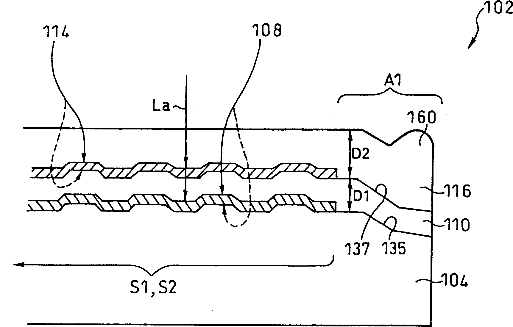
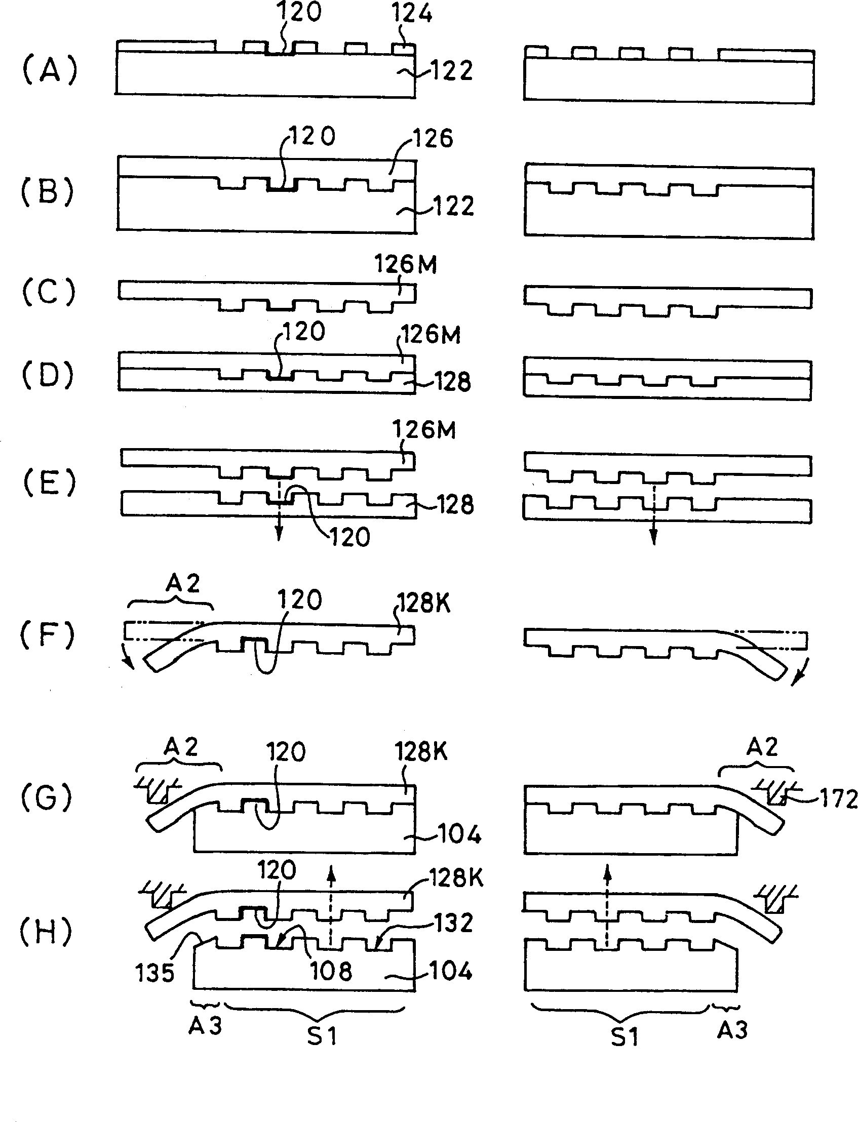
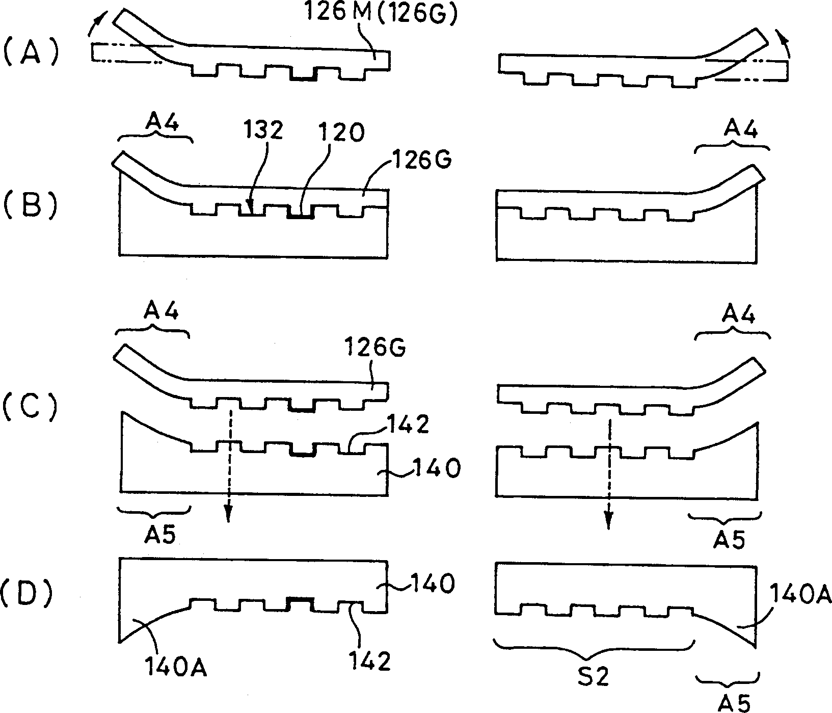
[0100] Here, a description will be given of an experimental example of preventing the occurrence of swelling on the upper surface of the second light-transmitting layer 116 by utilizing the curved shape of the outer peripheral portion (outer portion) of each layer.
[0101] In this experiment, the substrate 104 and the resin stamper 140 were produced by injection molding (as already described). The master stamper 128K for substrates and the original stamper or sub-mold 126G for resin stampers mounted on the molding dies 160 and 180 are for groove recording and have a track pitch of 0.3 μm.
[0102]For the substrate 104, polycarbonate resin (H4000-N282 manufactured by Mitsubishi Engineering Plastics) is used, the mold temperature is 125° C., the resin melting temperature is 360° C., and the mold clamping force is 35 tons to make a substrate 104 with an outer diameter of 12 cm and a thickness of 1.1 mm. .
[0103] On the other hand, the resin stamper 140 adopts olefin resin (ZE...
Embodiment 2
[0112] For comparison, according to the experiment conducted by the inventors in parallel with the experiment related to the above-mentioned Example 1, except for the combination of the substrate (104) and the resin stamper (140) whose outer peripheral portion is flat (no bending pattern is formed), according to An optical disc (102) was produced under the same conditions as in Example 1 above, and the outermost raised portion (160) protruded 60 μm from the surface of the second light-transmitting layer 116 corresponding to the information recording area (S2). In this state, the optical disc (102) may collide with a laser detector for reading and writing (not shown in the figure), and some kind of post-processing is required.
[0113] However, for example if Figure 8 As shown, this problem can be solved by forming a size R1 somewhat larger than the final product of the optical disc 202 itself, and then cutting off the outer peripheral portion A8 other than the predetermined s...
PUM
| Property | Measurement | Unit |
|---|---|---|
| thickness | aaaaa | aaaaa |
| thickness | aaaaa | aaaaa |
| thickness | aaaaa | aaaaa |
Abstract
Description
Claims
Application Information
 - R&D
- Intellectual Property
- Life Sciences
- Materials
- Tech Scout
- Unparalleled Data Quality
- Higher Quality Content
- 60% Fewer Hallucinations
Browse by: Latest US Patents, China's latest patents, Technical Efficacy Thesaurus, Application Domain, Technology Topic, Popular Technical Reports.
© 2025 PatSnap. All rights reserved.Legal|Privacy policy|Modern Slavery Act Transparency Statement|Sitemap|About US| Contact US: help@patsnap.com