

Film transistor array panel with visual checking device and its checking method
A thin-film transistor and panel technology, applied in the field of visual inspection, can solve problems such as difficult to obtain laser cutting space, difficult laser cutting, etc.
- Summary
- Abstract
- Description
- Claims
- Application Information
AI Technical Summary
Problems solved by technology
Method used
Image


Examples
Embodiment Construction
[0039] A thin film transistor (TFT) will be described with reference to the drawings.
[0040] figure 1 are circuit diagrams according to the first and second embodiments of the present invention.
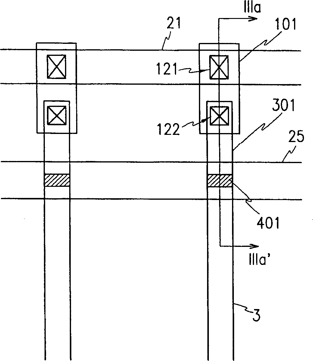
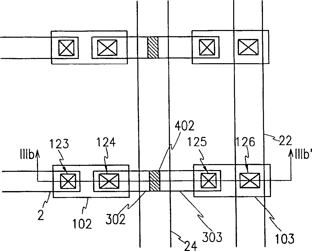
[0041] A plurality of gate lines 2 extend laterally, and a plurality of data lines 3 insulated to cross the gate lines 2 in a longitudinal direction are formed on an insulating substrate 100 . A plurality of gate pads 20 connected to the gate driver IC are connected to the first end of the gate line 2, and a plurality of data pads 30 connected to the data driver IC are connected to the second end of the data line 3 . The gate lines 2 and the data lines 3 cross each other to define pixel areas, and a group of pixel areas forms a display area. A portion other than the display area is defined as the surrounding area. A gate TFT B for inspection is connected to a third end opposite to the gate line 2 , and a data TFT A for inspection is connected to a fourth end opposite to the sec...
PUM
 Abstract
Description
Claims
Application Information