Organic thin film transistor
A technology of organic thin film and organic thin film layer, applied in the field of organic TFT, which can solve the problems of insufficient on/off ratio, slow action speed, and insufficient compound performance, etc.
- Summary
- Abstract
- Description
- Claims
- Application Information
AI Technical Summary
Problems solved by technology
Method used
Image
Examples
Embodiment approach 1
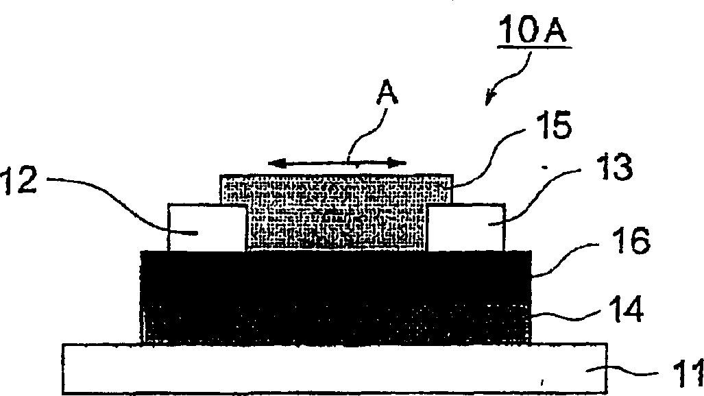
[0018] Such as figure 1 As shown, the organic TFT 10A of the present embodiment has a field effect transistor (FET: Field Effect Transistor) structure. The organic TFT 10A includes a source electrode (first electrode) 12 and a drain electrode (second electrode) 13 separated by a certain distance, an organic thin film layer (organic compound layer) 15 respectively connected to the electrodes 12 and 13, and separated from the electrodes 12 and 13 respectively. Control electrode (third electrode) 14 at a certain distance, and control the current flowing between the source / drain electrodes 12 and 13 according to the voltage applied to the control electrode 14 .
[0019]That is, on the substrate 11 of the organic TFT 10A, a gate electrode (layer) 14 and an insulator layer (gate insulating layer) 16 are sequentially formed, and an active electrode 12 and a drain electrode 13 are formed on the insulator layer 16 with a certain distance therebetween. An organic thin film layer 15 is ...
Embodiment approach 2
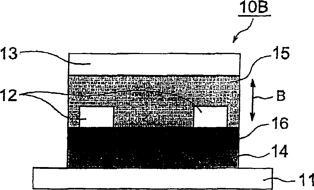
[0042] figure 2 It is a sectional view showing the structure of the organic TFT 10B of this embodiment. The organic TFT also has a FET structure, including a source electrode 12 and a drain electrode 13 separated by a certain distance, an organic thin film layer 15 connected to the electrodes 12 and 13 respectively, and a control electrode 14 separated from the electrodes 12 and 13 by a certain distance.
[0043] That is, in this organic TFT 10B, a control electrode 14 and an insulator layer 16 are provided in this order on a substrate 11 , and a pair of source electrodes 12 and 12 are provided on the insulator layer 16 with a certain distance therebetween. The organic thin film layer 15 is formed on the exposed surface of the insulator layer 16 including the pair of source electrodes 12 and 12 , and the drain electrode 13 is formed on the organic thin film layer 15 . In this organic TFT 10B, the organic thin film layer 15 also has a channel region, and the voltage applied t...
Embodiment approach 3
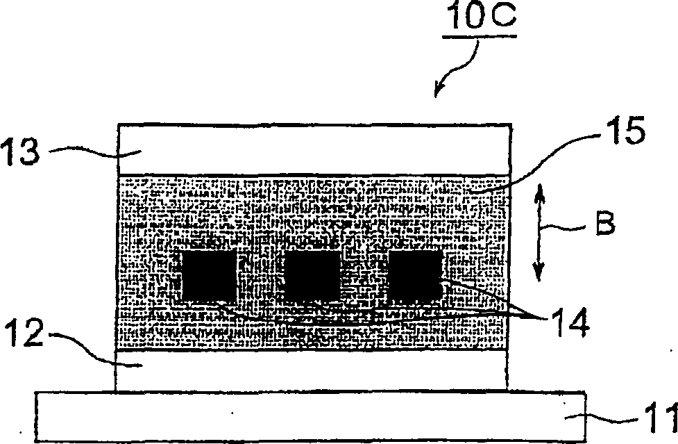
[0046] image 3 It is a cross-sectional view showing the structure of the organic TFT 10C of the present embodiment. This organic TFT 10C has a static induction transistor (SIT: Static Induction Transistor) structure. The organic TFT 10C includes a source electrode 12 and a drain electrode 13 separated by a certain distance, an organic thin film layer 15 connected to the electrodes 12 and 13 respectively, and a control electrode 14 separated from the electrodes 12 and 13 by a certain distance.
[0047] That is, in this organic TFT 10C, a source electrode 12 , an organic thin film layer 15 , and a drain electrode 13 are sequentially provided on a substrate 11 , and a set of three control electrodes 14 is provided in the organic thin film layer 15 . The control electrode 14 extends inwardly of the paper and is parallel to the source electrode 12 and the drain electrode 13 respectively.
[0048] In the above-mentioned organic TFT 10C, the organic thin film layer 15 also has a c...
PUM
| Property | Measurement | Unit |
|---|---|---|
| Film thickness | aaaaa | aaaaa |
| Film thickness | aaaaa | aaaaa |
| Thickness | aaaaa | aaaaa |
Abstract
Description
Claims
Application Information


