Storage circuit with test compression function
A storage circuit and circuit technology, applied in the field of storage circuits, can solve the problem of reducing the recovery rate of waste elements, etc.
- Summary
- Abstract
- Description
- Claims
- Application Information
AI Technical Summary
Problems solved by technology
Method used
Image

Examples
no. 1 example
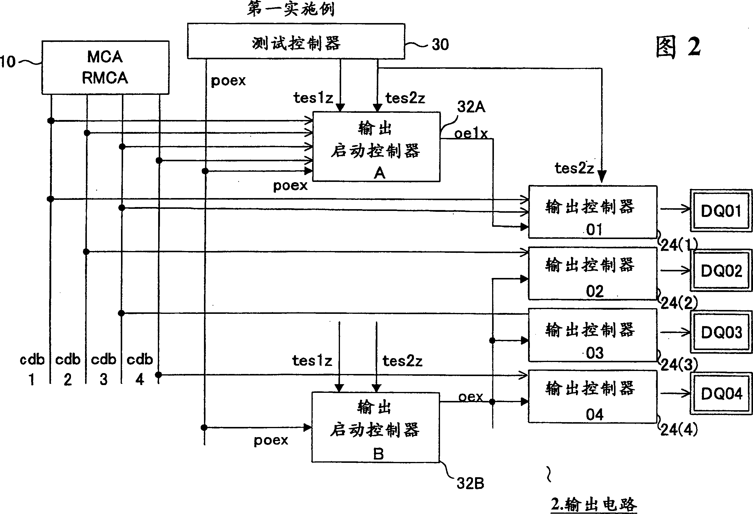
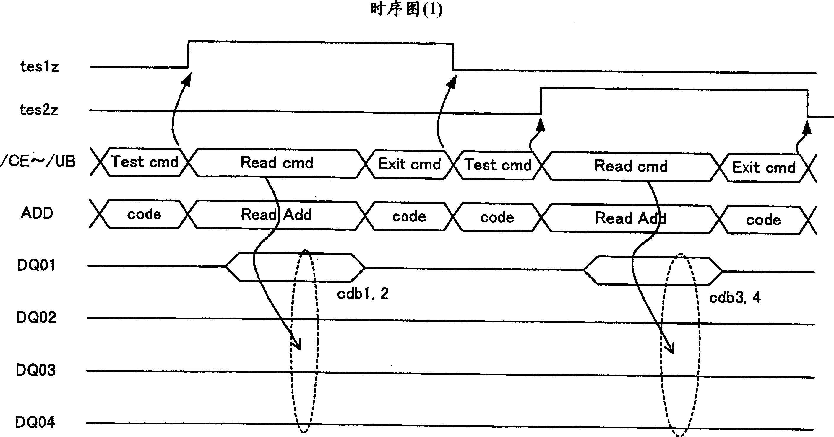
[0033] FIG. 2 is a configuration diagram of an output circuit of the first embodiment, image 3 is a timing chart of the test mode of the first embodiment. As an example, this embodiment is a 4-bit output structure. In the test mode, 2 bits are compressed and tested at the same time, and two sets of compressed outputs are serially output from the first input / output terminal DQ1.
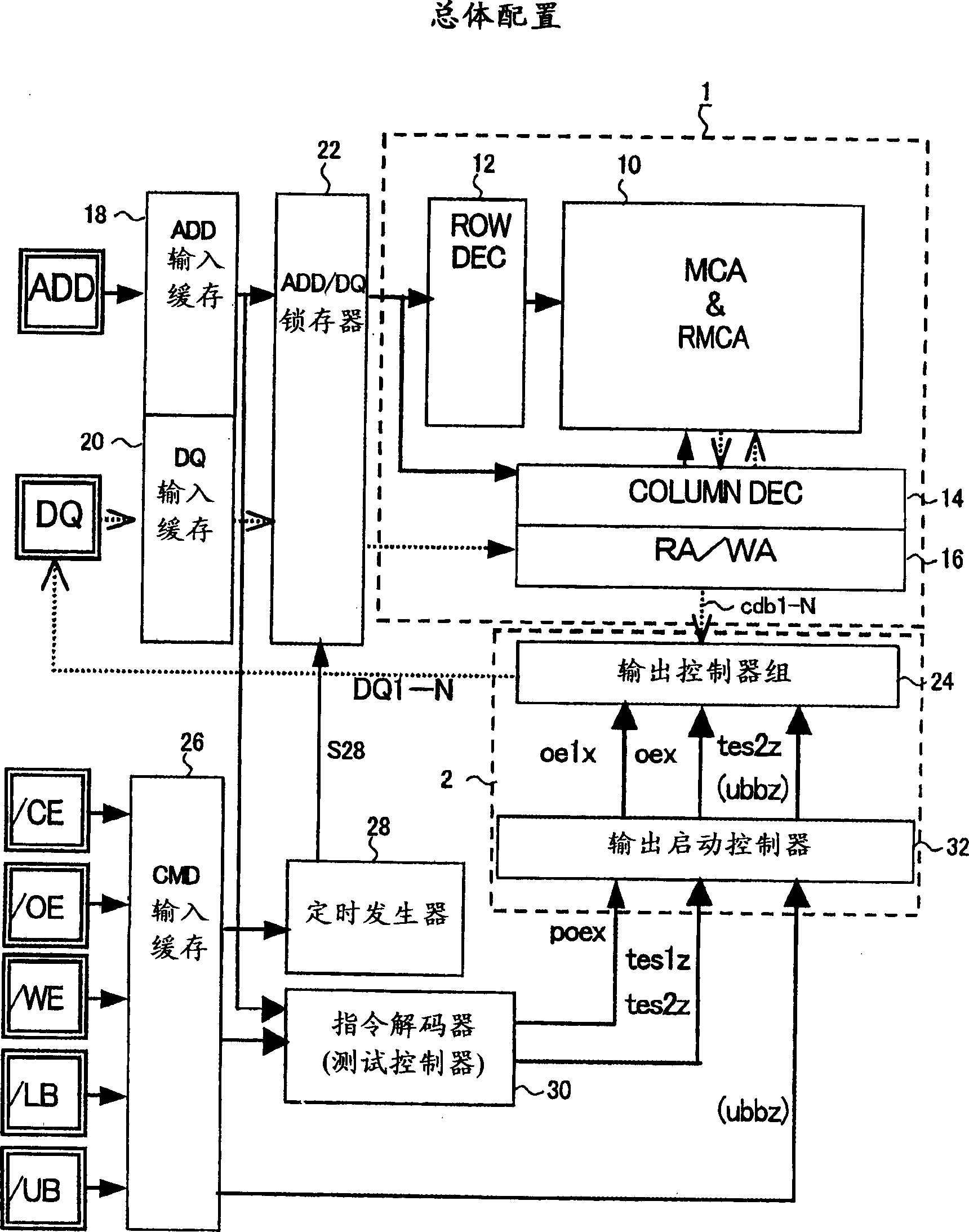
[0034] As shown in FIG. 2, 4-bit output data is output from 4-bit common data buses cdb1 to cdb4 at the element array 10 constituting the memory core. The 4-bit data on the common data bus is latched in the figure 1shown in the sense amplifier RA. In addition, the common data bus is shared by many memory cores, and the 4-bit output of the selected memory core is output to the common data bus.
[0035] The 4-bit common data buses cdb1 to cdb4 are connected to the 4 output control circuits 24, respectively. Also, the four output control circuits 24 are connected to the four input / output terminals D...
no. 2 example
[0052] FIG. 8 is a configuration diagram of an output circuit of the second embodiment, and Figure 9 is an operation timing chart of this embodiment. For the second preferred embodiment, in response to a test command sent from the outside, the test control circuit 30 sets the test control signal tes1z to a high level. The result is to enter test mode. The high byte signal / UB then directly controls the selection of the two compression test outputs. In other words, if the high byte signal / UB is low, the first test mode is entered, and the compressed output signals of the common data buses cdb1 and cdb2 are output to the output terminal DQ1. If the high byte signal / UB is high, the second test mode is entered, and the compressed output signals of the common data buses cdb3 and cdb4 are output to the output terminal DQ1. For this selection method of the compression test output signal, in the test mode, as long as the external signal is not used as a read command, any externa...
PUM
 Abstract
Description
Claims
Application Information
 - R&D
- Intellectual Property
- Life Sciences
- Materials
- Tech Scout
- Unparalleled Data Quality
- Higher Quality Content
- 60% Fewer Hallucinations
Browse by: Latest US Patents, China's latest patents, Technical Efficacy Thesaurus, Application Domain, Technology Topic, Popular Technical Reports.
© 2025 PatSnap. All rights reserved.Legal|Privacy policy|Modern Slavery Act Transparency Statement|Sitemap|About US| Contact US: help@patsnap.com