Integrated structure of array waveguide grating and optical fiber array and manufacture method thereof

A technology of arrayed waveguide grating and optical fiber array, which is applied in the directions of optical waveguide light guide, coupling of optical waveguide, light guide, etc., can solve the problems of complicated manufacturing process and increased cost of AWG devices

Inactive Publication Date: 2003-06-11
INST OF SEMICONDUCTORS - CHINESE ACAD OF SCI
View PDF0 Cites 44 Cited by
  • Summary
  • Abstract
  • Description
  • Claims
  • Application Information

AI Technical Summary

Problems solved by technology

However, the fabrication process of these two waveguides is complex and significantly increases the cost of AWG devices

Method used


Image

  • Integrated structure of array waveguide grating and optical fiber array and manufacture method thereof
  • Integrated structure of array waveguide grating and optical fiber array and manufacture method thereof
  • Integrated structure of array waveguide grating and optical fiber array and manufacture method thereof

Examples


Embodiment Construction

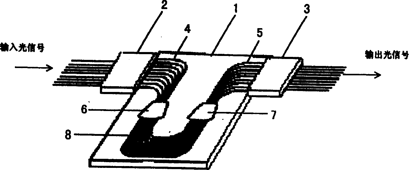
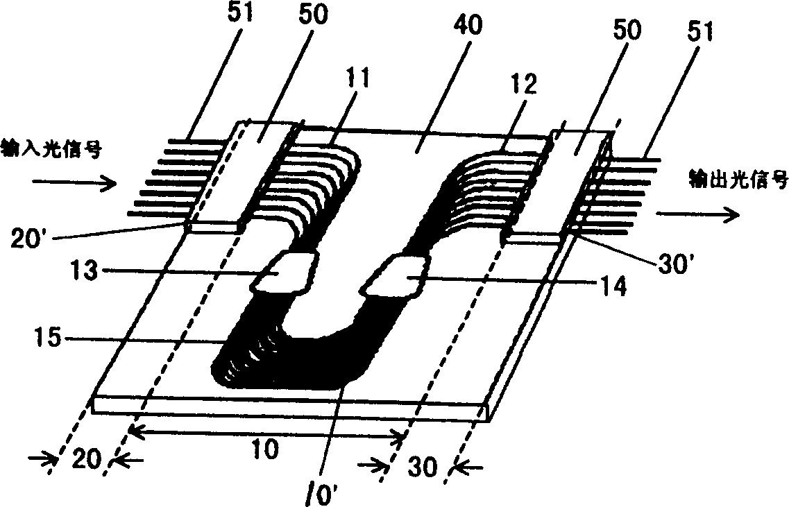
[0030] see figure 2 It is a perspective view illustrating the integrated structure of an arrayed waveguide grating and an optical fiber array according to an embodiment of the present invention. In the case shown in the figure, the number of channels of the optical fiber array is 8, and there will be 16 channels, 32 channels, 64 channels, 128 channels, etc. in practical applications. Such as figure 2 As shown, the structure includes a substrate 40 and two upper covers 50 , and input and output multi-core single-mode optical fibers 51 bonded between the substrate 40 and the upper covers 50 .

[0031] Wherein, the substrate 40 is divided into three areas: the AWG area 10, the input fiber array area 20 and the output fiber array area 30, which are formed on the same silicon substrate. figure 1 Three discrete optical passive devices are integrated together.

[0032]The arrayed waveguide grating is formed in the AWG area 10, and its function is to multiplex or demultiplex the ...


PUM


Abstract

The structure comprises the array of the wave-guide grating as well as the input and output optical fiber array, which is aimed at and coupled to the array of the input and output wave-guide in the array of the wave-guide grating. The array of the wave-guide grating and the input and output optical fiber array are integrated on the same silicon substrate. The self-alignment method is adopted in the invention to carry out the end surface coupling between the input and output wave-guide in the array of the wave-guide grating and the optical fiber array. The optical fiber array is prepared by using the adhesive agent to bond the array of the V or U shaped groove on the substrate, the upper cover piece and the monomode fiber with multiple cores.

Description

technical field [0001] The present invention is an integrated structure of the arrayed waveguide grating and the fiber array, especially the structure that can make the input / output waveguide of the arrayed waveguide grating directly aligned with the fiber array easily. The invention also relates to a method for manufacturing the integrated structure, and a process for manufacturing the optical waveguide in the arrayed waveguide grating. Background technique [0002] Dense Wavelength Division Multiplexing (DWDM) technology is an effective method to solve broadband and large-capacity optical fiber network communication. Multiplexing / demultiplexing is a key component in constructing a DWDM system. At present, there are generally three technologies for realizing wavelength division multiplexing (WDM), which are arrayed waveguide grating (AWG), fiber grating (FBG) and other interference filter devices (Filter). High reliability, large number of channels, flat passband, and exc...

Claims


Application Information

Patent Timeline
Patent Type & Authority Applications(China)
IPC IPC(8): G02B6/12G02B6/13G02B6/26G02B6/30G02B6/34
Inventor 刘育梁贺月娇
Owner INST OF SEMICONDUCTORS - CHINESE ACAD OF SCI
Why Eureka
Try Eureka