Integrated structure of array waveguide grating and optical fiber array and manufacture method thereof
A technology of arrayed waveguide gratings and fiber arrays, applied in the direction of optical waveguide light guides, optical waveguide coupling, etc., can solve the problems of complex manufacturing process and increased cost of AWG devices
- Summary
- Abstract
- Description
- Claims
- Application Information
AI Technical Summary
Problems solved by technology
Method used
Image
Examples
Embodiment Construction
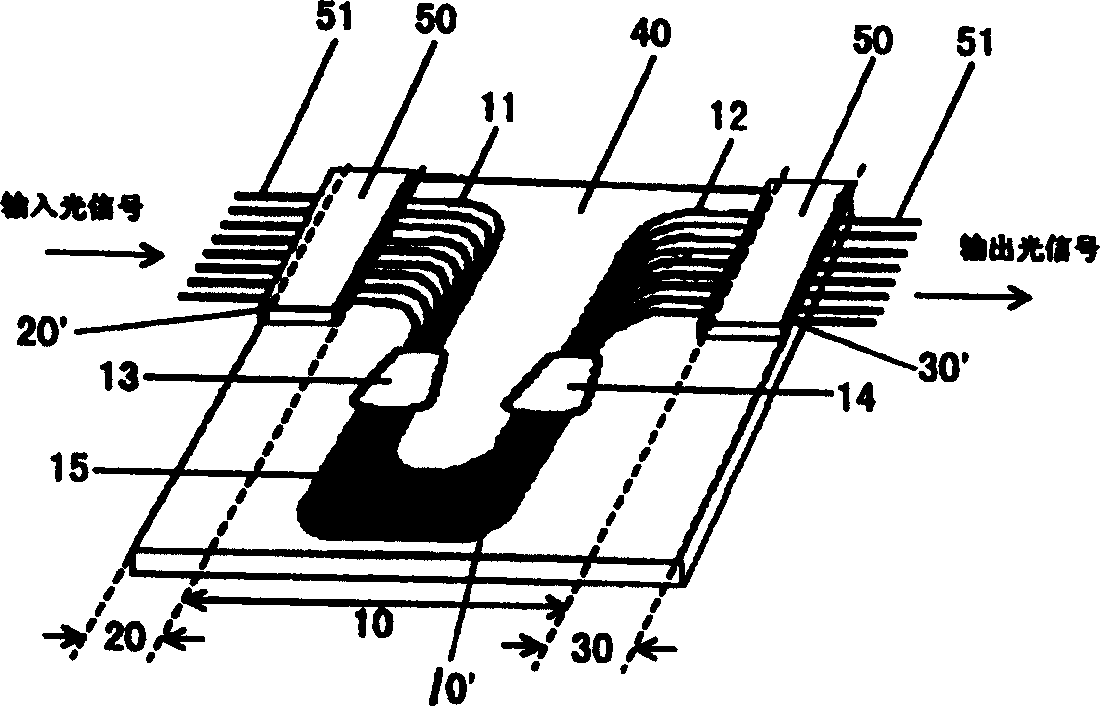
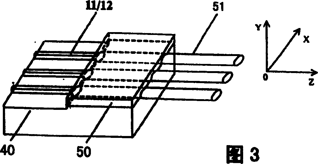
[0030] see figure 2 It is a perspective view illustrating the integrated structure of an arrayed waveguide grating and an optical fiber array according to an embodiment of the present invention. In the case shown in the figure, the number of channels of the optical fiber array is 8, and there will be 16 channels, 32 channels, 64 channels, 128 channels, etc. in practical applications. Such as figure 2 As shown, the structure includes a substrate 40 and two upper covers 50 , and input and output multi-core single-mode optical fibers 51 bonded between the substrate 40 and the upper covers 50 .
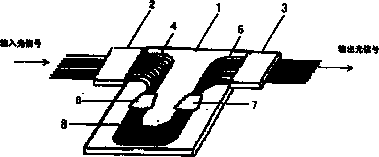
[0031] Wherein, the substrate 40 is divided into three areas: the AWG area 10, the input fiber array area 20 and the output fiber array area 30, which are formed on the same silicon substrate. figure 1 Three discrete optical passive devices are integrated together.
[0032]The arrayed waveguide grating is formed in the AWG area 10, and its function is to multiplex or demultiplex the ...
PUM
 Abstract
Description
Claims
Application Information


