Electrode material, dielectric material and plasma display front panel
A technology of dielectric material and display panel, which is applied in alternating current plasma display panels, dielectric/insulating layers, gas discharge electrodes, etc., and can solve problems such as PDP image quality deterioration.
- Summary
- Abstract
- Description
- Claims
- Application Information
AI Technical Summary
Problems solved by technology
Method used
Image

Examples
experiment example 1
[0065] Experimental Example 1: Electrode Glue
[0066] Ethyl cellulose as a resin and α-terpineol as a solvent were stirred and mixed at a weight mixing ratio of 4:6 to prepare a solution containing an organic component. After that, the solution, Ag powder and glass powder having the composition shown in Table 1 (average particle size 1.5 μm, maximum particle size 4.5 μm) were mixed in a weight ratio of 30:3:67, mixed and dispersed with three rollers , prepare the electrode glue.
[0067] Evaluation
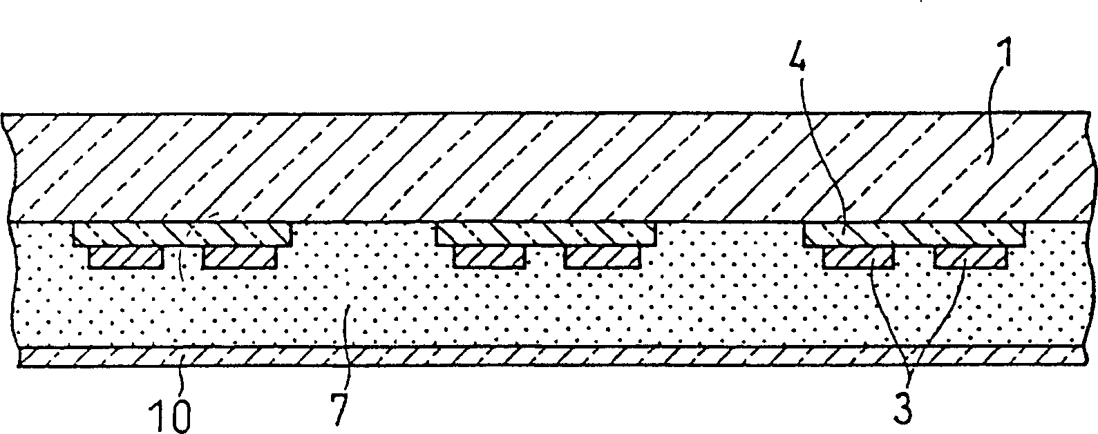
[0068] ① All the electrode pastes obtained above were formed into unpatterned film electrodes, coated on a glass substrate (PP8, manufactured by Nippon Electric Glass Co., Ltd.) by a blade coating method, and dried at 90°C for 30 minutes. After sintering at 580°C for 10 minutes, the obtained electrode thickness was 10 μm.
[0069] The cross-cut method (JES K5600-5-6) was used to evaluate the bonding strength of the electrodes. In this evaluation, the case where the cut edge i...
experiment example 2
[0075] Experimental Example 2: Electrode Glue
[0076] An electrode paste was prepared in the same manner as in Experimental Example 1, except that the glass powder having the composition, average particle diameter, and maximum particle diameter shown in Table 2 was used, and the adhesion strength and yellowing degree were evaluated in the same manner. The results are shown in Table 2.
[0077] 1
[0078] It can be seen from Table 2 that when the average particle size of the glass powder contained in the electrode paste is less than 4.0 microns and the maximum particle size is less than 10 microns, the bonding strength between the formed electrode and the glass substrate is strengthened, and the yellowing of the PDP can be reduced.
experiment example 3
[0079] Experimental example 3: Dielectric glue
[0080] Ethyl cellulose as a resin and α-terpineol as a solvent were stirred and mixed at a weight mixing ratio of 5:30 to prepare a solution containing an organic component. Then, the solution was mixed with glass powder having the compositions shown in Tables 3 and 4 (average particle size: 2 μm, maximum particle size: 8 μm) at a weight ratio of 65:35, mixed and dispersed with three rolls, and prepared out the dielectric glue.
[0081] Evaluation
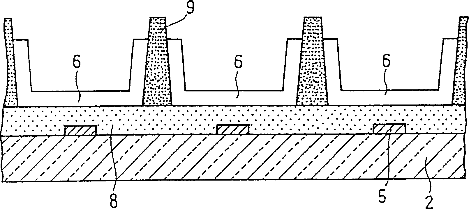
[0082] ① The above-obtained dielectric paste was applied to a glass substrate having an electrode prepared using the electrode paste of the present invention by a blade coating method, dried at 90°C for 30 minutes, and then fired at 580°C for 10 minutes. The resulting electrode thickness was 40 microns.
[0083] The b value representing the degree of coloration of the glass substrate was measured using a colorimeter. The value obtained by subtracting the b value of Ag itself and th...
PUM
| Property | Measurement | Unit |
|---|---|---|
| The average particle size | aaaaa | aaaaa |
| Particle size | aaaaa | aaaaa |
| Thickness | aaaaa | aaaaa |
Abstract
Description
Claims
Application Information
 - R&D
- Intellectual Property
- Life Sciences
- Materials
- Tech Scout
- Unparalleled Data Quality
- Higher Quality Content
- 60% Fewer Hallucinations
Browse by: Latest US Patents, China's latest patents, Technical Efficacy Thesaurus, Application Domain, Technology Topic, Popular Technical Reports.
© 2025 PatSnap. All rights reserved.Legal|Privacy policy|Modern Slavery Act Transparency Statement|Sitemap|About US| Contact US: help@patsnap.com