Test equipment for packed semiconductor elements

A technology for packaging components and testing devices, applied in the field of semiconductor packaging component testing devices, can solve the problems of inaccurate testing, residual spring probes, poor contact, etc., and achieve the effect of avoiding poor contact

Inactive Publication Date: 2003-08-20
SILICON INTEGRATED SYSTEMS
View PDF0 Cites 6 Cited by
  • Summary
  • Abstract
  • Description
  • Claims
  • Application Information

AI Technical Summary

Problems solved by technology

However, after using for a period of time, the spring probe will have problems such as oxidation and residual tin slag, resulting in poor contact, so it will cause errors in the test, which will affect the test results.
Taking BGA Package Device as an example, its pins are solder balls, so when the above-mentioned spring probes are used for testing, there will be tin slag of solder balls remaining on the spring probes. In the next test, it will not be able to test accurately due to poor contact

Method used


Image

  • Test equipment for packed semiconductor elements
  • Test equipment for packed semiconductor elements
  • Test equipment for packed semiconductor elements

Examples


Embodiment Construction

[0045] The semiconductor packaging device testing device according to the preferred embodiment of the present invention will be described below with reference to the related drawings, wherein the same components will be described with the same reference symbols.

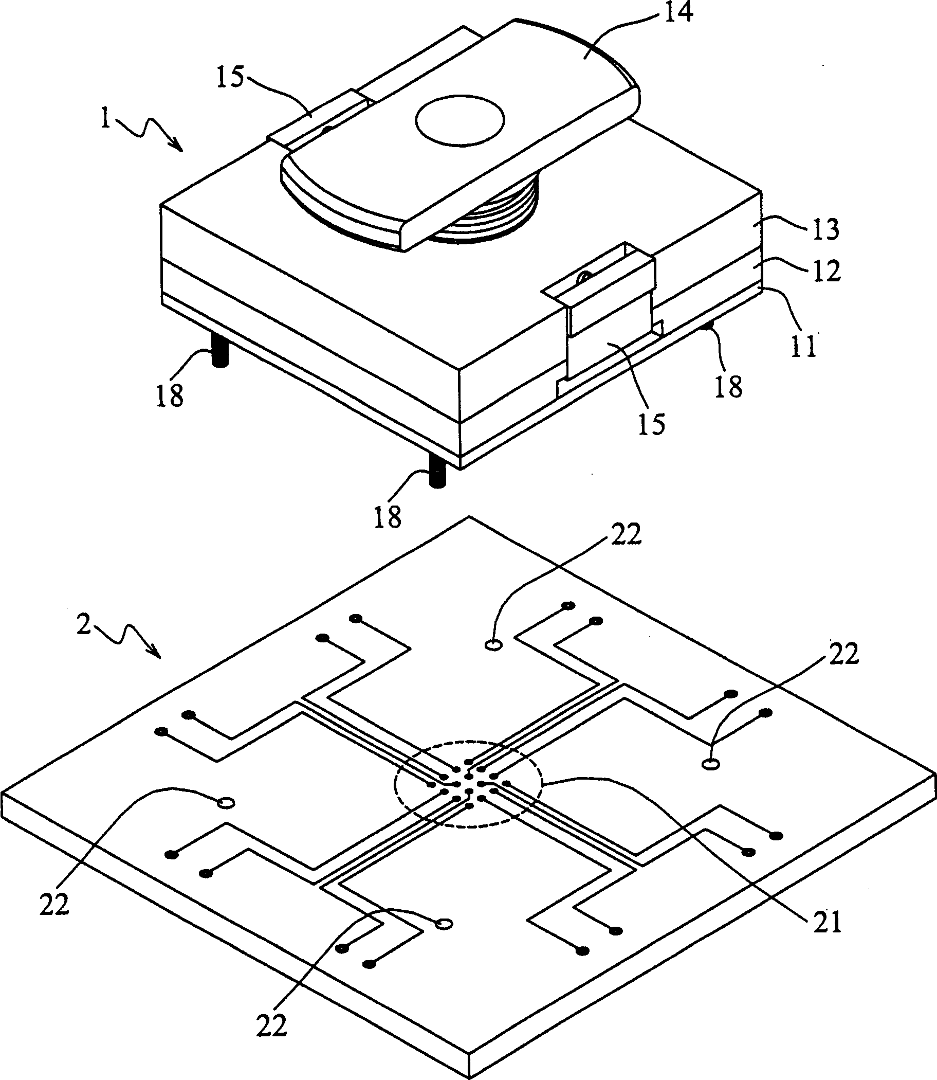
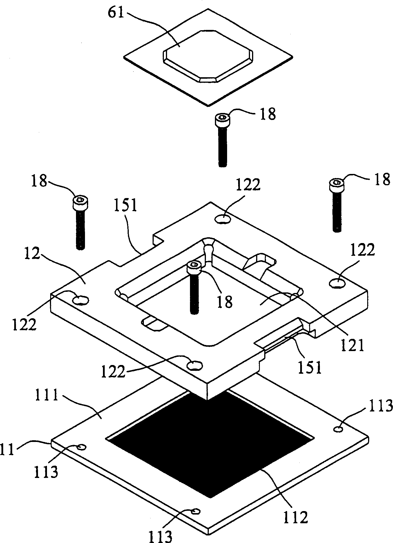
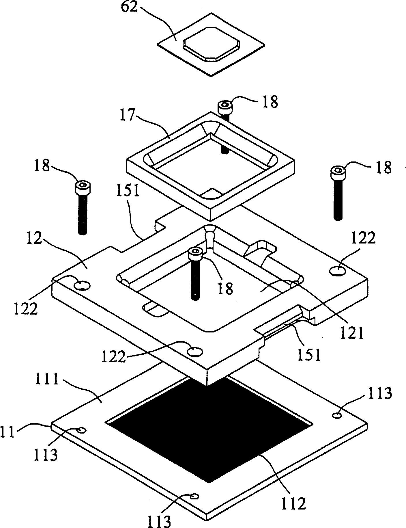
[0046] Please refer to figure 1 As shown, the semiconductor package device testing device 1 according to the preferred embodiment of the present invention includes a conductive element 11 , a first body 12 , a second body 13 , a pressing member 14 , and a bonding portion 15 .

[0047] The semiconductor package component testing device 1 cooperates with a test board (load board) 2 to test the semiconductor package component.

[0048] In this embodiment, the conductive element 11 has a frame portion 111 and a conductive film 112, the conductive film 112 can be an elastic conductive film, and a plurality of conductive points (such as figure 2 As shown), the material of these conductive points is a metal with good cond...


PUM


Abstract

The test equipment for semiconductor packing element includes one conducting element, one first main body, one second main body and one pressing member. The conducting element on one side of the first main body has several conducting points for containing the pins of the packed semiconductor element electrically; the first main body has one first port to form one space to hold the semiconductor packing element; the second main body is on the other side of the first main body; and the pressing member locates the semiconductor packing element in the first port and is connected to the second main body. The present invention is suitable for manual test of semiconductor packing element of different sizes and has excellent electrical contact owing to the conducting element.

Description

technical field [0001] The invention relates to a semiconductor packaging component testing device, in particular to a semiconductor packaging component testing device applied to manual testing. Background technique [0002] Generally speaking, IC chips must be tested after being packaged to ensure the quality of the semiconductor packaged components. In order to adapt to the large increase in production volume of current semiconductor factories, it is more efficient to use automated testing equipment to test semiconductor packaging components. [0003] However, for some special situations, such as product development testing, a small number of product verification, testing product electrical properties, etc., if a set of automated testing equipment is specially set up for these special situations, the cost will be too high; Using test devices to deal with these special situations will stop the production line, cause waste, and cause trouble for testers, because testers may...

Claims


Application Information

Patent Timeline
Patent Type & Authority Applications(China)
IPC IPC(8): G01R31/26G01R31/28H01L21/66
Inventor 廖沐盛谢宜璋周秀竹
Owner SILICON INTEGRATED SYSTEMS
Why Eureka
Try Eureka