Capacitance type fingerprint access chip

A fingerprint reading and capacitive technology, which is applied in character and pattern recognition, instruments, computer components, etc., can solve the problems of reducing the quality of output fingerprint signals, and cannot provide methods to prevent electrostatic damage, and achieve complete development and maturity. The effect of improving production yield and reducing cost

Inactive Publication Date: 2003-10-22
EGIS TECH
View PDF6 Cites 87 Cited by
  • Summary
  • Abstract
  • Description
  • Claims
  • Application Information

AI Technical Summary

Problems solved by technology

[0005] However, the main disadvantage of this charge and discharge reading method is that it is necessary to control the characteristics of the fixed current discharge MOS (controlled by the external current mirror Current Mirror) of each capacitive sensing element on the chip to be consistent in order to obtain a good output s

Method used


Image

  • Capacitance type fingerprint access chip
  • Capacitance type fingerprint access chip
  • Capacitance type fingerprint access chip

Examples


Embodiment Construction

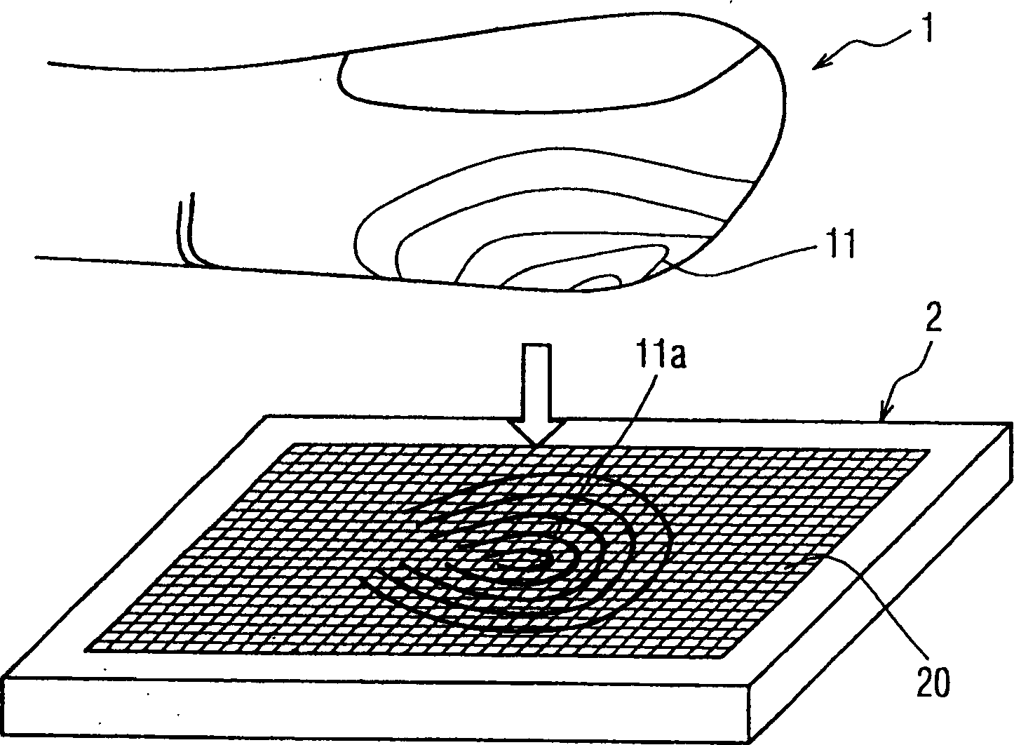
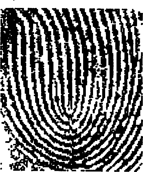
[0069] See figure 1 , which is a schematic diagram of using the capacitive fingerprint reading chip of the present invention as finger fingerprint reading. Wherein the fingerprint reading chip 2 includes: a plurality of capacitive sensing elements 20 arranged in a two-dimensional (2-D) array, when the finger 1 touches the chip 2, the irregular-shaped ridge (Ridge) 11 on the surface of the finger 1 will be Contact with part of the capacitive sensing element 20, and leave the capacitance curve 11a corresponding to the peak 11 on the device 2. By reading the shape of the capacitance curve 11a, the shape of the original fingerprint peak 11 can be identified, for example Figure 1a Shown is the binary fingerprint image actually read by the capacitive fingerprint reading chip of the present invention, which is used to prove the innovative implementation of the present invention.

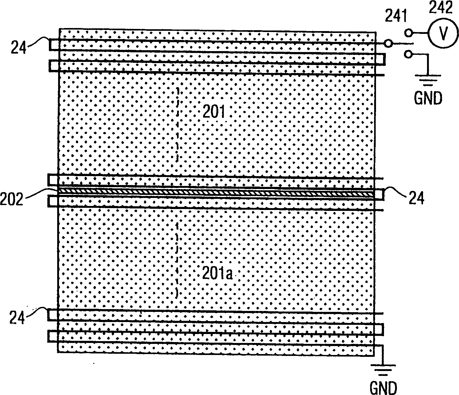
[0070] to understand more clearly figure 1 The structure of the capacitive fingerprint reading chip s...


PUM

PropertyMeasurementUnit
Thicknessaaaaaaaaaa

Abstract

The invention is a capacitance fingerprint access chip, it includes capacitance sensing array which is arranged with planar type and a dynamic random access memory peripheral circuit. The device usesDRAM charge sharing theory to examine the apex and the vale of the fingerprint. The peripheral circuit outputs the result of each capacitance sensor. The manufacturing method belongs to integrate circuit craft, especially the CMOS craft. The invention can be biological identification of people, applies to notebook PC, personal digital assistant and mobile.

Description

technical field [0001] The invention relates to a capacitive fingerprint reading chip, in particular to a capacitive fingerprint reading chip using a dynamic random access memory data reading structure. Background technique [0002] In the existing fingerprint reading method, the oldest method is to press the ink with the finger, emboss it on the paper, and then use optical scanning to input it into the computer and compare it with the fingerprint pattern in the database. The biggest disadvantage is that it cannot achieve the purpose of real-time processing. Therefore, it is impossible to meet more and more demands for real-time authentication, such as: network authentication, e-commerce, confidentiality of portable electronic products, IC card personal identity authentication, security system and so on. [0003] Real-time fingerprint reading methods have become a key technology in the biometrics market. The traditional real-time fingerprint reading is optical. Please refer...

Claims


Application Information

Patent Timeline
IPC IPC(8): G06K9/62
Inventor 周正三张世彬郑元伟
Owner EGIS TECH
Why Eureka
Try Eureka