

Semiconductor device
A technology of semiconductors and devices, applied in the field of semiconductor devices, can solve the problems of occupying chip space, conductors occupying RAM space, etc.
- Summary
- Abstract
- Description
- Claims
- Application Information
AI Technical Summary
Problems solved by technology
Method used
Image

Examples
Embodiment Construction
[0018] Preferred embodiments of the present invention are described below with reference to the accompanying drawings.
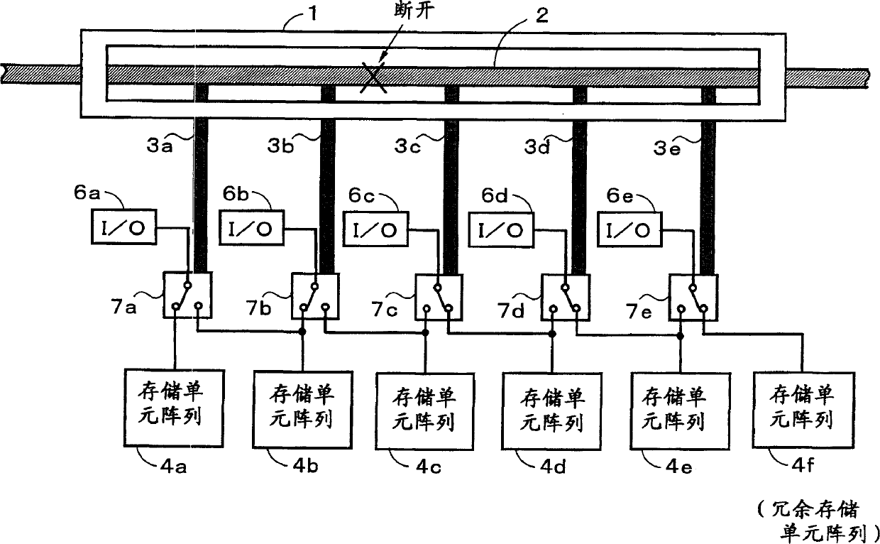
[0019] FIG. 1 is a schematic diagram showing the structure of a semiconductor device according to a first embodiment of the present invention. As shown in FIG. 1, a semiconductor device has a rectangular guard ring 1, a fuse pattern 2 extending in a direction parallel to the longitudinal axis of the guard ring 1, and patterns 3a-3e are branched from the fuse pattern 2, and The retainer 1 is drawn out in a direction perpendicular to the longitudinal axis of the retainer 1 . The semiconductor device also has a plurality of memory cell arrays 4a-4e, each corresponding to input / output (I / O) ports 6a-6e for receiving and sending memory signals. Here an additional memory cell array 4f is provided for repairing memory defects found after manufacture if necessary. Switching circuits 7a-7e switch connections between I / O ports 6a-6e and memory cell arrays 4e-4f, sel...
PUM
 Abstract
Description
Claims
Application Information