High-voltage bootstrap diode composite device structure

A composite device, high-voltage bootstrapping technology, applied in diodes, semiconductor devices, electro-solid devices, etc., can solve the problems of device size and increase in manufacturing cost, and achieve the effects of reducing power consumption, saving chip space, and reducing leakage current

Active Publication Date: 2020-07-14
UNIV OF ELECTRONIC SCI & TECH OF CHINA
View PDF9 Cites 2 Cited by
  • Summary
  • Abstract
  • Description
  • Claims
  • Application Information

AI Technical Summary

Problems solved by technology

All in all, the current optimization scheme based on the traditional bootstrap diode implementation method still has a lot of room for i

Method used


Image

  • High-voltage bootstrap diode composite device structure
  • High-voltage bootstrap diode composite device structure
  • High-voltage bootstrap diode composite device structure

Examples


Embodiment 1

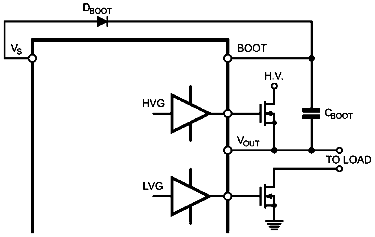
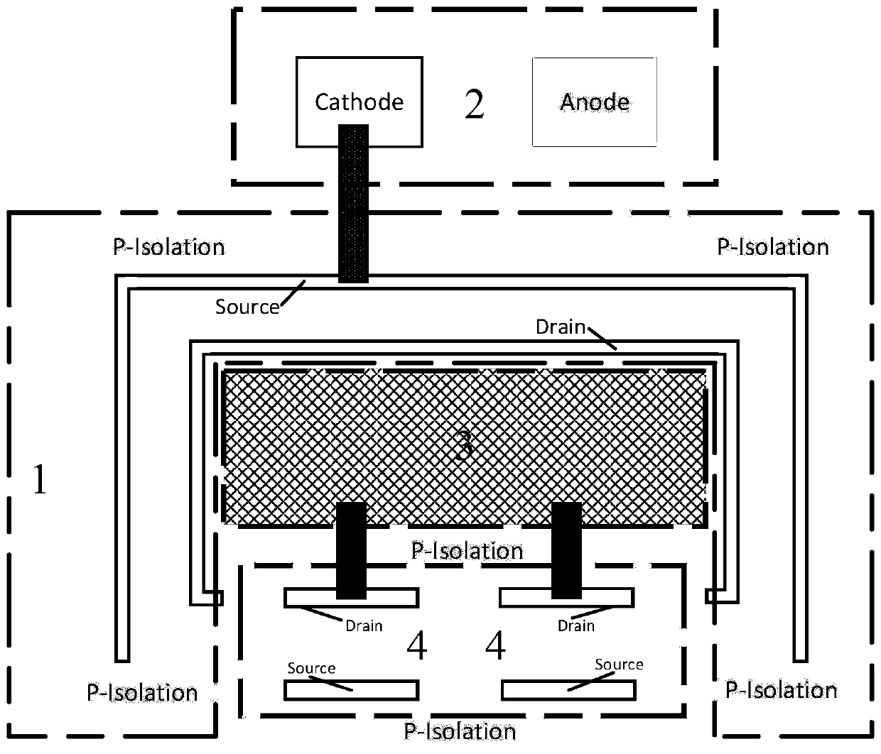
[0024] This embodiment provides a high-voltage bootstrap diode composite device structure, the composite device includes a high-voltage JFET and a diode device, and the source of the high-voltage JFET is connected to the cathode of the diode through metal, thereby forming a composite device that can replace a traditional high-voltage bootstrap diode.

[0025] In terms of layout, the high-voltage JFET device 1 is surrounded by P-type isolation P-Isolation, so that the JFET forms a ring-like structure. At the same time, in order to facilitate the connection with the diode, the JFET outer ring side is the JFET source region Source, and the inner ring side is the JFET drain region Drain. Diode 2 is also surrounded by P-type isolation, and the cathode Cathode is connected to the source of JFET1 through metal to form a composite device, which can be combined with two Divided RESURF structures or Self Shielded structure LDMOS4 for level shifting to form a high-side circuit ring island...

Embodiment 2

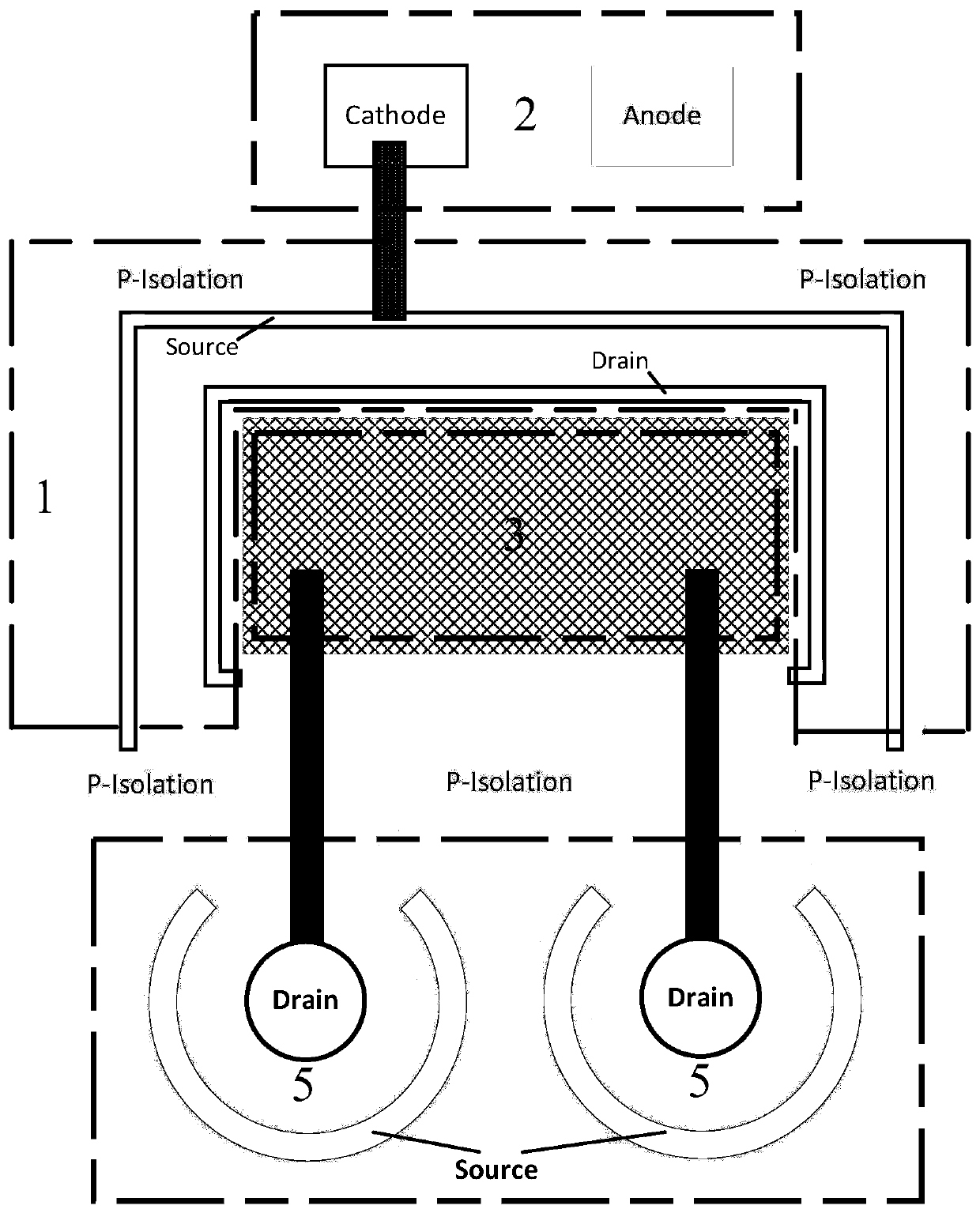
[0032] Such as Figure 5 As shown, the difference between this embodiment and Embodiment 1 is that the high-voltage JFET device 1 is formed by the second P-type buried layer 112, the second P-type implantation P-TYPE111, and the second P-type well region P-WELL110 In the through isolation structure, the second P-type implanted P-TYPE 111 part extends in the X direction to align with the end of the second P-type buried layer 112 to adjust the pinch-off voltage of the JFET.

Embodiment 3

[0034] Such as Figure 6 As shown, the difference between this embodiment and Embodiment 1 is that the high-voltage JFET device 1 is formed by the second P-type buried layer 112, the second P-type implantation P-TYPE111, and the second P-type well region P-WELL110 In the via isolation structure, the length of the second P-type buried layer 112 in the X direction is consistent with that of the second P-type well region P-WELL 110 .


PUM


Abstract

The invention proposes a high-voltage bootstrap diode composite device structure, with which, under the conditions that the chip area is saved, low leakage current is guaranteed and a control circuitis not additionally arranged, the high-voltage withstand characteristic is met, the composite device can effectively replace a bootstrap diode in a high-voltage gate drive chip, and the function of the bootstrap diode is achieved and optimized. The composite device structure consists of a high-voltage JFET and a diode and can be used in a level shift module of a high-side circuit of a high-voltagegate drive circuit, and a source electrode of the JFET is connected with a cathode of the diode through metal, so the high-voltage bootstrap diode composite device is formed. In the aspect of layout,the composite device is combined with an LDMOS of a partition RESURF structure or a self-shielding structure for level shift to form a high-side circuit roundabout, the high-side circuit roundabout and a high-voltage circuit in the roundabout form a high-side circuit, and the high-side circuit roundabout and the high-voltage circuit jointly control on-off of a high-side power transistor.

Description

technical field [0001] The invention belongs to the technical field of power semiconductor devices, and relates to a composite device structure for replacing a bootstrap diode of a high-voltage gate drive circuit. Background technique [0002] Due to their excellent characteristics such as fast switching speed and high withstand voltage, power semiconductor devices gradually occupy the ranks of core devices in the electronics manufacturing industry. Power field effect transistors are also favored in realizing high-speed switching, and the control circuits of such devices, such as In the half-bridge gate drive circuit, the bootstrap module effectively solves the compatibility problem of the high and low voltage circuits. The module consists of a bootstrap diode and a bootstrap capacitor. The performance of the bootstrap diode is crucial to the performance of the entire drive circuit. Simply connecting the diode outside the chip will increase the cost of the chip, while the in...

Claims


Application Information

Patent Timeline
IPC IPC(8): H01L27/06H01L27/02H01L29/06
CPCH01L27/0629H01L27/0207H01L29/0638H01L29/0646H01L29/0615H01L29/0634
Inventor 乔明李贺珈袁章亦安张波
Owner UNIV OF ELECTRONIC SCI & TECH OF CHINA
Why Eureka
Try Eureka