Semiconductor device

A technology of semiconductors and devices, applied in the field of semiconductor devices, can solve the problems of occupying chip space, conductors occupying RAM space, etc.

Inactive Publication Date: 2005-07-13
FUJITSU SEMICON LTD
View PDF0 Cites 0 Cited by
  • Summary
  • Abstract
  • Description
  • Claims
  • Application Information

AI Technical Summary

Problems solved by technology

However, the fuse pattern structure of Figure 7(A) takes up a lot of chip space because each fuse requires space for one window and retainer
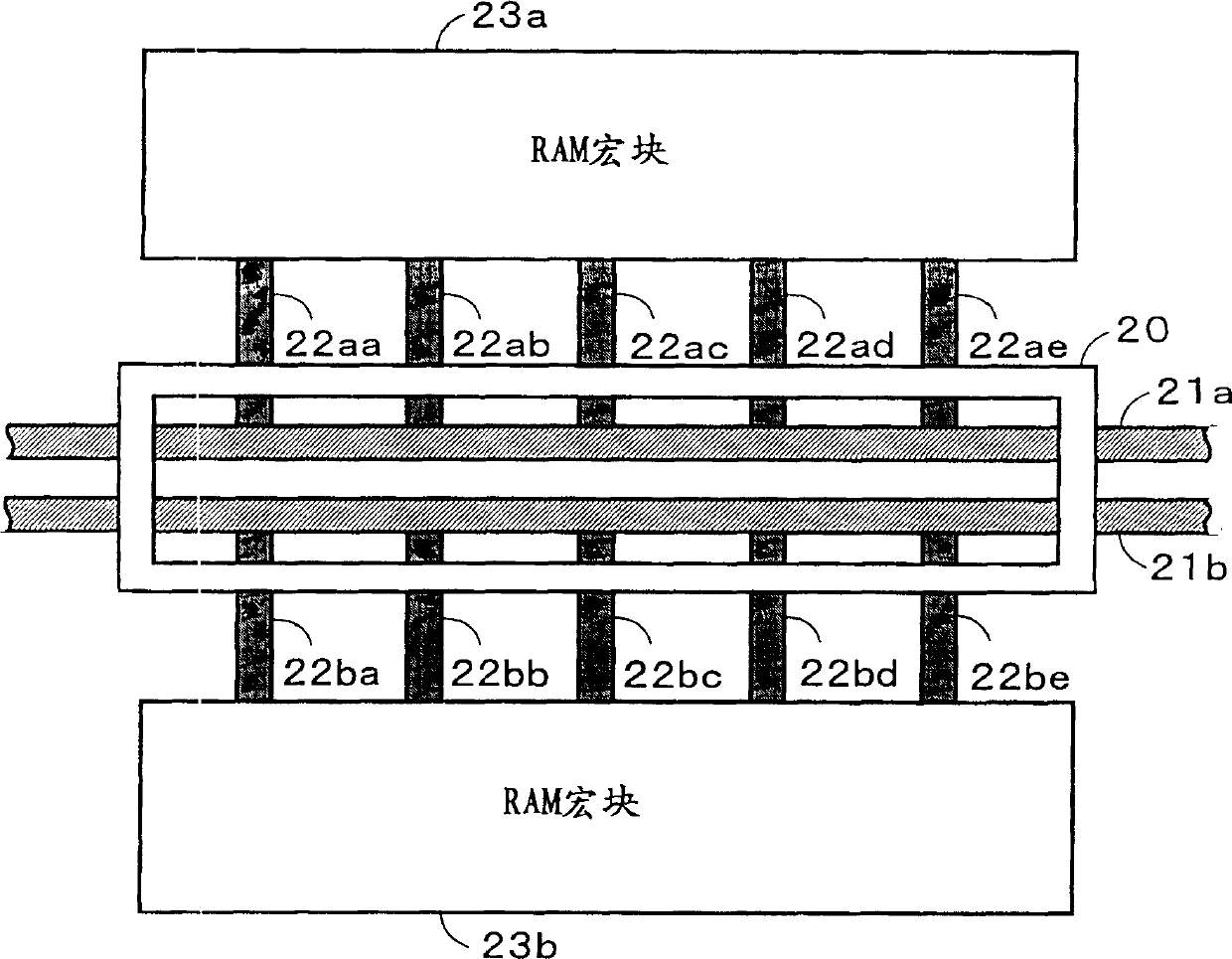
Although the structure of Fig. 7(B) is more efficient than Fig. 7(A) in terms of fuse and retainer area, the conductors connecting each fuse pattern to the RAM macroblock occupy RAM space
In addition, since each fuse pattern should be long enough to receive the laser beam at two different points, there is a limit to the reduction of the dimension in the length direction indicated by the double-headed arrow (A) shown in FIG. 7(B). Small

Method used


Image

  • Semiconductor device
  • Semiconductor device
  • Semiconductor device

Examples


Embodiment Construction

[0018] Preferred embodiments of the present invention are described below with reference to the accompanying drawings.

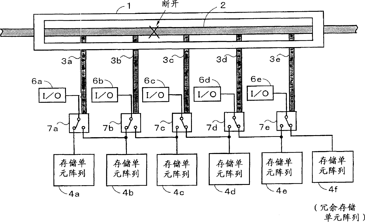
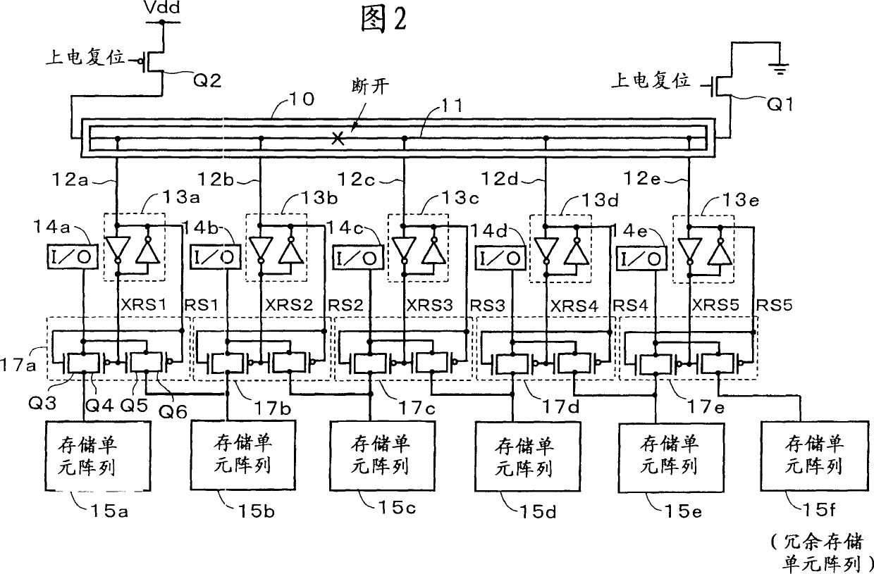
[0019] FIG. 1 is a schematic diagram showing the structure of a semiconductor device according to a first embodiment of the present invention. As shown in FIG. 1, a semiconductor device has a rectangular guard ring 1, a fuse pattern 2 extending in a direction parallel to the longitudinal axis of the guard ring 1, and patterns 3a-3e are branched from the fuse pattern 2, and The retainer 1 is drawn out in a direction perpendicular to the longitudinal axis of the retainer 1 . The semiconductor device also has a plurality of memory cell arrays 4a-4e, each corresponding to input / output (I / O) ports 6a-6e for receiving and sending memory signals. Here an additional memory cell array 4f is provided for repairing memory defects found after manufacture if necessary. Switching circuits 7a-7e switch connections between I / O ports 6a-6e and memory cell arrays 4e-4f, sel...


PUM


Abstract

A semiconductor device with a laser-programmable fuse for repairing memory defects discovered after fabrication, where the guard ring and fuse pattern are designed to take up less chip space. The semiconductor device has a fuse pattern extending parallel to a longitudinal axis of a rectangular retainer, and patterns branching from the fuse pattern and drawn out from the retainer in a direction perpendicular to the axis. The semiconductor device also has a plurality of memory cell arrays, each of which is connected to an I / O port for receiving and sending memory signals. One of these arrays is used as an array of memory cells for repair purposes. The device further has a switch circuit for switching the connection between the I / O port and the memory cell array, selecting the defective memory cell array of the I / O port or their adjacent memory cells including redundant memory cells array.

Description

technical field [0001] The present invention relates to a semiconductor device, and more particularly, to a semiconductor device having a fuse for repairing defects found after manufacture. Background technique [0002] A semiconductor device including memory circuits has a redundant memory array for repairing memory defects found after manufacture. The repair process disconnects the defective memory cell array from other circuits by blowing laser programmable fuses provided in the device, and restores its functionality with the now activated redundant array. In this chip structure, the fuse patterns are respectively disposed under rectangular guard rings, so that the laser beams irradiated inside the guard rings will irradiate the desired fuse patterns. 6(A) and (B) illustrate guard ring and fuse patterns formed in one semiconductor device. Specifically, FIG. 6(A) is a plan view, and FIG. 6(B) is a cross-sectional view taken along line 100-100 in FIG. 6(A). [0003] As s...

Claims


Application Information

Patent Timeline
Patent Type & Authority Patents(China)
IPC IPC(8): H01L21/82G11C17/14G11C29/00
CPCG11C17/14G11C17/143G11C29/812G11C29/848G11C29/00
Inventor 牧康彦
Owner FUJITSU SEMICON LTD
Why Eureka
Try Eureka