

Organic field effect transistor
An organic field and transistor technology, applied in the field of organic field effect transistors, can solve problems such as non-solution and impractical, and achieve the effect of easy material selection
- Summary
- Abstract
- Description
- Claims
- Application Information
AI Technical Summary
Problems solved by technology
Method used
Image

Examples
example 1
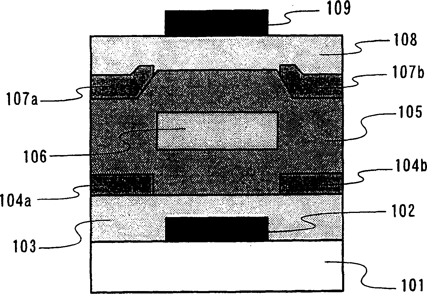
[0091] In this example, it will be specified Figure 1B The organic FET shown in . First, a 50 nm thick gold film was formed on a glass substrate by vacuum evaporation through a mask having a first gate electrode pattern. Thus, a first gate electrode having a length of 500 μm on each side was formed.
[0092] Move the glass substrate to a chemical evaporation device. Xylylene Dimer (xylylene dimer) (product name: parylene, parylene manufactured by Parylene Japan) was heated under reduced pressure, and a heating tube heated to 680° C. was inserted for pyrosis. Therefore, radicals were generated Monomer. The generated radical monomer was introduced onto the substrate kept at room temperature to form a 300 nm thick polyparaxylylene film. This is the first gate insulating film.
[0093] Next, in order to form the first source electrode and the first drain electrode, a mask pattern was provided so that the length of the source-drain was 50 μm. Thus, a 50 nm-thick gold thin film...
example 2
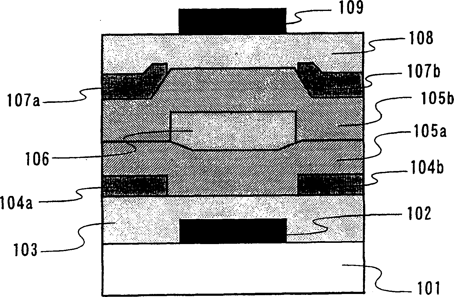
[0101] In this example, the specific Figure 1B The organic FET shown in . First, a 50 nm thick gold film was formed on a glass substrate by vacuum evaporation through a mask having a first gate electrode pattern. Thus, a first gate electrode having a length of 500 μm on each side was formed.
[0102] Move the glass substrate to a chemical evaporation device. Xylylene Dimer (xylylene dimer) (product name: parylene, parylene manufactured by Parylene Japan) was heated under reduced pressure, and a heating tube heated to 680° C. was inserted for burning. Thus, a radical monomer was generated. The generated radical monomer was introduced onto the substrate kept at room temperature to form a 300 nm thick polyparaxylylene film. This is the first gate insulating film.
[0103] Next, in order to form the first source electrode and the first drain electrode, a mask pattern was provided so that the length of the source-drain could be 50 μm. Thus, a 50 nm-thick gold thin film was for...
example 3
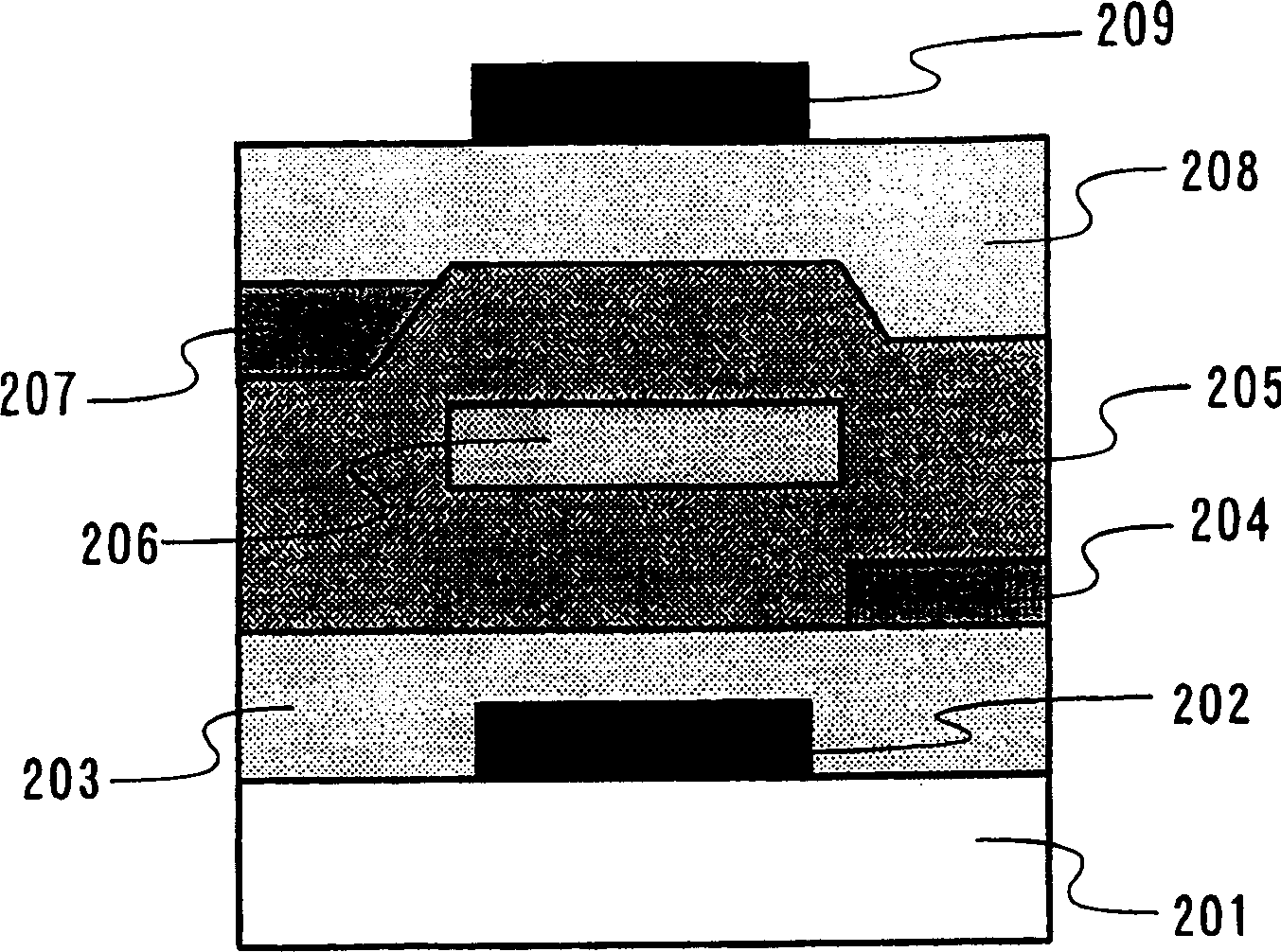
[0111] In this example, it will be specified Figure 1B The organic FET shown in . First, a 50 nm thick gold film was formed on a glass substrate by vacuum evaporation through a mask having a first gate electrode pattern. Thus, a first gate electrode having a length of 500 μm on each side was formed.
[0112] Move the glass substrate to a chemical evaporation device. Xylylene Dimer (xylylene dimer) (product name: parylene, parylene manufactured by Parylene Japan) was heated and evaporated under reduced pressure, and a heating tube heated to 680° C. was inserted for burning. Thus, a radical monomer was generated .The generated free radical monomer is introduced onto the substrate kept at room temperature to form a 300nm thick polyparaxylylene film. This is the first gate insulating film.
[0113] Next, in order to form the first source electrode and the first drain electrode, a mask pattern was provided so that the length of the source-drain could be 50 μm. Thus, a 50 nm-thic...
PUM
| Property | Measurement | Unit |
|---|---|---|
| thickness | aaaaa | aaaaa |
Abstract
Description
Claims
Application Information