Method for manufacturing thin-film structure

A manufacturing method and structure technology, which is applied in semiconductor/solid-state device manufacturing, microstructure technology, microstructure devices, etc., can solve the problem of stress difference between corrosion film and substrate, and achieve the effect of improving soft melting

Inactive Publication Date: 2003-12-17
MITSUBISHI ELECTRIC CORP
View PDF0 Cites 1 Cited by
  • Summary
  • Abstract
  • Description
  • Claims
  • Application Information

AI Technical Summary

Problems solved by technology

[0004] However, when the corrosion film is formed of a TEOS oxide film as in the prior art, there is a problem that a stress difference occurs between the corrosion film and the substrate during thermal shrinkage.

Method used


Image

  • Method for manufacturing thin-film structure
  • Method for manufacturing thin-film structure
  • Method for manufacturing thin-film structure

Examples


Embodiment approach 1

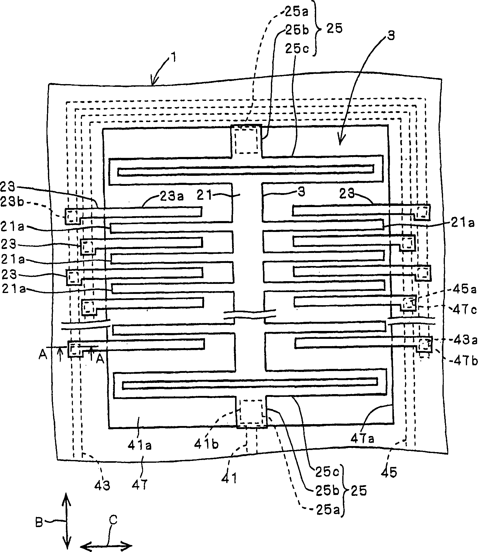
[0022] Such as figure 1 and figure 2 As shown, the semiconductor acceleration sensor manufactured by applying the thin film structure manufacturing method according to Embodiment 1 of the present invention has a substrate 1 as a sensor substrate, and a sensor unit 3 formed on the substrate 1 and having a function of detecting acceleration.

[0023] Sensor part 3 such as figure 1 As shown, there are a mass body 21 functioning as a movable electrode, a plurality of fixed electrodes 23 , and a plurality of beams 25 . Mass body 21 , fixed electrode 23 , and beam 25 correspond to the thin film body of the present invention, and are formed of doped polysilicon obtained by doping a conductive material such as polysilicon with impurities such as phosphorus.

[0024] The mass body 21 is arranged at a predetermined interval from the substrate 1 and has a plurality of movable electrode portions 21 a extending in a direction C perpendicular to the direction B of the detected accelerati...

Embodiment approach 2

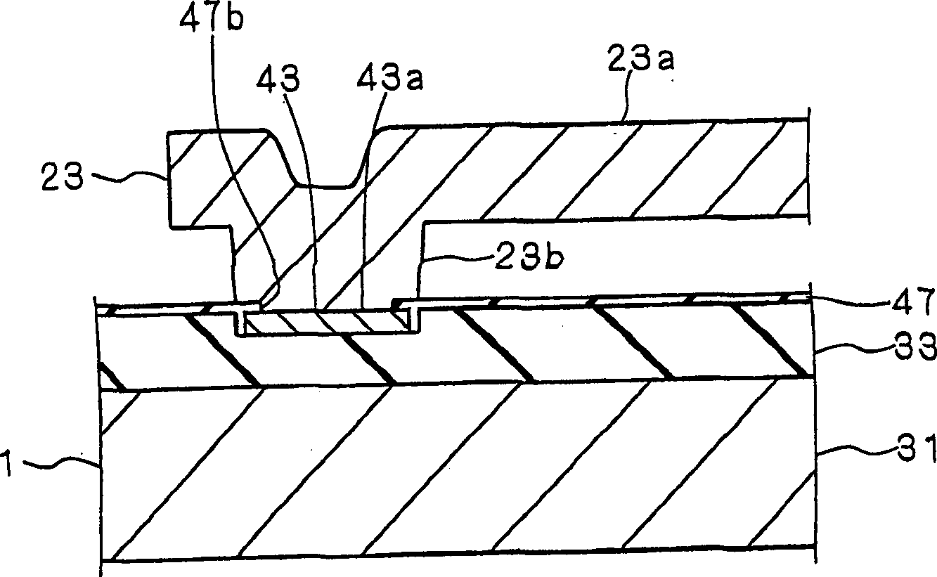
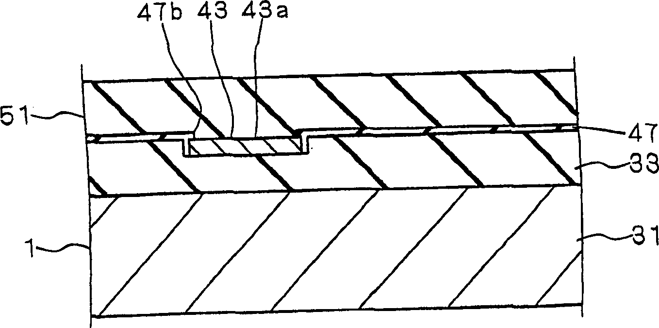
[0038] The manufacturing method of the thin film structure according to this embodiment is also applicable to figure 1 and figure 2 The semiconductor acceleration sensor shown. In addition, the substantial difference between the manufacturing method according to the present embodiment and the manufacturing method according to the above-mentioned first embodiment lies in the difference in the method of manufacturing the etching film 51 . Therefore, here, only the substantial differences between the manufacturing method according to this embodiment and the manufacturing method according to Embodiment 1 will be described.

[0039]In the manufacturing method according to the present embodiment, the etching film 51 is formed of a BPSG (borophosphosilicateglass) film of a silicon oxide film whose phosphorus concentration is set within a predetermined range. In this embodiment, the concentration of phosphorus in the BPSG film is also set to a value greater than 3 mol % and less th...


PUM


Abstract

The present invention relates to a manufacturing method of a thin-film structural body which is formed by using a semiconductor processing technique, and an object thereof is to provide a manufacturing method of a thin-film structural body, capable of reducing a stress difference exerted between a sacrifice film and a substrate upon thermal shrinkage.In order to achieve this object, a sacrifice film (51), which is formed on a substrate (1), is formed by using a PSG film in which the concentration of phosphorus is set to a value which is greater than 3 mol %, and also smaller than 4 mol %. After a thin-film layer (53) has been formed thereon and after the thin-film layer (53) has been patterned, the sacrifice film (51) is removed by an etching process.

Description

technical field [0001] The present invention relates to a method of manufacturing a thin film structure having a substrate and a thin film formed on an etched film formed on the substrate and disposed at a predetermined interval from the substrate by removing the etched film. Background technique [0002] In the thin film structure applicable to the present invention, due to the difference in thermal shrinkage properties between the substrate and the corrosion film, for example, after the corrosion film is formed and subjected to thermal baking treatment, a stress difference will be generated between the substrate and the corrosion film. Poorness can sometimes cause cracks in the substrate or the corrosion film or both the substrate and the corrosion film. [0003] In the manufacturing method of the existing thin-film structure body related to this, be to form TEOS (tetraethylorthosilicate, tetraethylorthosilicate) oxide film on the substrate as corrosion film, after forming...

Claims


Application Information

Patent Timeline
Patent Type & Authority Applications(China)
IPC IPC(8): B81B3/00G01P15/08G01P15/125H01L21/306H01L29/84
CPCG01P2015/0814B81B2203/0118G01P15/0802B81C1/00365B81C2201/0109B81B2203/0136G01P15/125H01L29/84
Inventor 奥村美香堀川牧夫石桥清志西上武文
Owner MITSUBISHI ELECTRIC CORP
Why Eureka
Try Eureka