

Method for correcting convex block outline
A bump, contour technology, applied in the direction of electrical components, semiconductor/solid-state device manufacturing, circuits, etc., can solve problems such as device impact
- Summary
- Abstract
- Description
- Claims
- Application Information
AI Technical Summary
Problems solved by technology
Method used
Image

Examples
no. 2 example
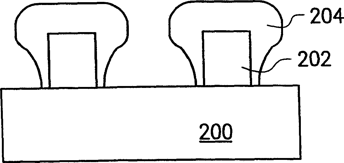
[0036] Figure 7 and Figure 8 As shown, it is a schematic cross-sectional view of forming a polymer material layer on the bump sidewall by a two-step deposition process according to the second embodiment of the invention.
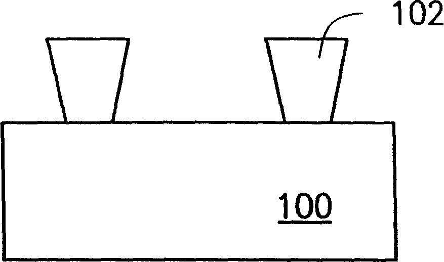
[0037] Please refer to Figure 7 and Figure 8 , a bump 202 has been formed on a substrate 200 . Wherein, the bump 202 may be a patterned photoresist layer or a patterned conductive layer.
[0038] Next, a two-step deposition process is performed to form a polymer material layer 208 on the sidewall of the bump 202 . Wherein, the present invention can control the growth of the polymer material layer 208 from the top of the sidewall of the bump 202 to the bottom of the sidewall of the bump 202 . The polymer material layer 208 can also be controlled to grow from the bottom of the sidewall of the bump 202 to the top of the sidewall of the bump 202 . In this embodiment, the polymer material layer 208 is formed by a plasma-enhanced chemical vapor depositio...
PUM
 Abstract
Description
Claims
Application Information