Semiconductor integrated circuit, signal transmitting device, electro-optical device, and electronic apparatus

A technology of integrated circuits and semiconductors, applied in the field of signal transmission devices, optoelectronic devices and electronic instruments, and semiconductor integrated circuits

Inactive Publication Date: 2004-01-14
SEIKO EPSON CORP
View PDF0 Cites 0 Cited by
  • Summary
  • Abstract
  • Description
  • Claims
  • Application Information

AI Technical Summary

Problems solved by technology

Although electrical signals are used for signal processing within the integrated circuit, the input and output with the outside of the integrated circuit are performed using optical signals.

Method used


Image

  • Semiconductor integrated circuit, signal transmitting device, electro-optical device, and electronic apparatus
  • Semiconductor integrated circuit, signal transmitting device, electro-optical device, and electronic apparatus
  • Semiconductor integrated circuit, signal transmitting device, electro-optical device, and electronic apparatus

Examples


no. 1 approach

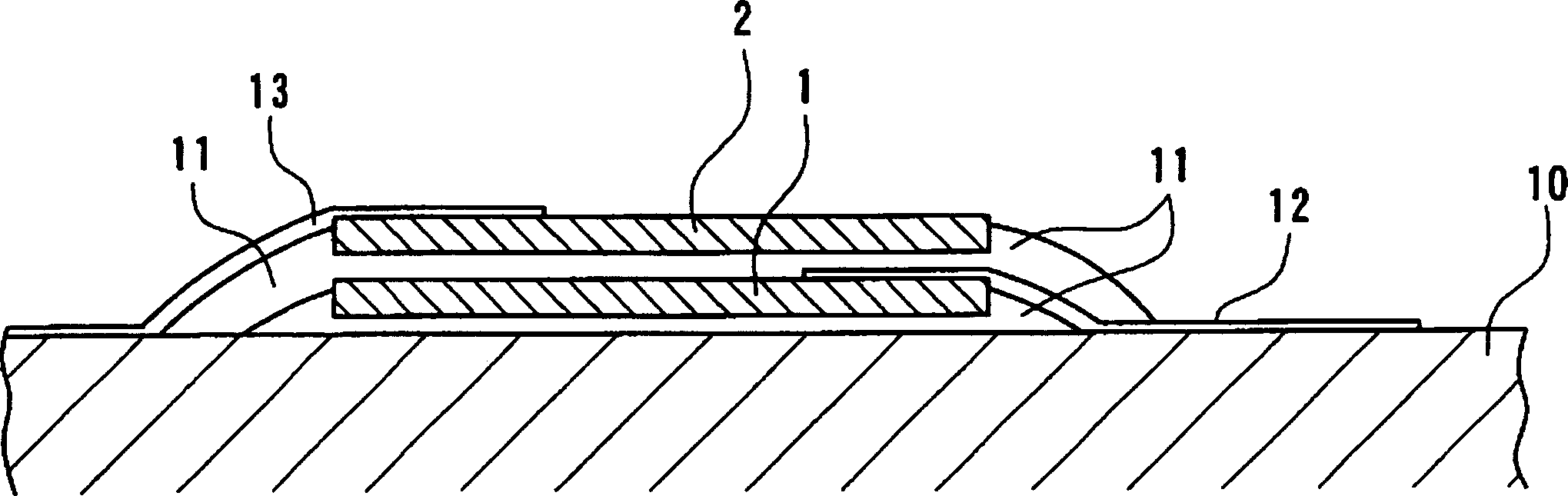
[0089] figure 1 is a schematic cross-sectional view of the semiconductor integrated circuit according to the first embodiment. figure 1 The semiconductor integrated circuit shown is composed of a substrate 10 , a microtile 1 and a microtile 2 .

[0090]The microtile-shaped element 1 and the microtile-shaped element 2 are microtile-shaped (plate-shaped) semiconductor devices, for example, quadrangular plate-shaped members with a thickness of 1 to 20 μm and a vertical and horizontal dimension of several tens of μm to hundreds of μm . The method of manufacturing the microtile-shaped element 1 and the microtile-shaped element 2 will be described later. In addition, the shape of the micro-tile-shaped element 1 and the micro-tile-shaped element 2 is not limited to a quadrangle, and may be other shapes.

[0091] The micro-tile-shaped component 1 and the micro-tile-shaped component 2 are overlapped and bonded by an adhesive 11 , and are pasted and fixed on one side of the substrate...

no. 2 approach

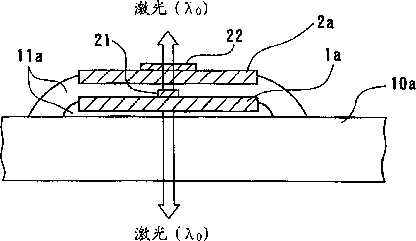
[0122] Below, refer to Figure 8 to Figure 12 A second embodiment of the present invention will be described. According to this embodiment, the two micro-tile-shaped elements that are superimposed and fixed on the substrate are light-emitting elements with different light-emitting wavelengths.

[0123] Figure 8 is a schematic cross-sectional view of the semiconductor integrated circuit according to the second embodiment. Figure 8 The illustrated semiconductor integrated circuit is composed of a substrate 10, a microtile 1a, and a microtile 1b.

[0124] Micro-tile-shaped element 1a and micro-tile-shaped element 1b and figure 1 The microtile-like element 1 shown has the microtile shape (plate shape) as well. Radiation laser light (wavelength λ 2 ) of the surface-emitting laser 21a, the micro-tile-shaped component 1b is provided with a radiating laser (wavelength λ 1 ) of the surface-emitting laser 21b. Moreover, the micro-tile-shaped element 1 a and the micro-tile-shaped ...


PUM


Abstract

The invention provides a semiconductor integrated circuit which allows a plurality of devices to be integrated compactly, that is, with high density; a signal transmitting device; an electro-optical device; and an electronic apparatus. A semiconductor integrated circuit includes tile-shaped microelements that are superimposed upon and adhered to the top surface of a substrate with an adhesive.

Description

technical field [0001] The invention relates to a semiconductor integrated circuit, a signal transmission device, a photoelectric device and an electronic instrument. In particular, it relates to a semiconductor integrated circuit, a signal transmission device, an electro-optical device, and an electronic instrument having a structure in which a plurality of micro-tile-like elements are overlapped and pasted together. Background technique [0002] On the silicon semiconductor substrate, set the surface emitting laser (VCSEL), photodiode (PD) and high electron mobility transistor (HEMT) made of gallium arsenide, or paste and fix the micro silicon transistor on the glass substrate, Thin-film transistors (TFTs) used to replace individual pixels of a liquid crystal display (LCD), these can be considered as technologies for forming semiconductor elements on substrates of different materials. [0003] As a semiconductor integrated circuit having such a different material, an opto...

Claims


Application Information

Patent Timeline
Patent Type & Authority Applications(China)
IPC IPC(8): H01L25/18H01L21/60H01L25/065H01L25/07H01L25/16H01L31/02H01S5/00H01S5/022H01S5/026H01S5/0683H01S5/183H01S5/40H01S5/42
CPCH01L2924/10329H01L24/83H01L24/29H01L2224/24225H01L2924/13064H01L2224/32225H01L2221/68368H01L2224/83001H01L24/24H01S5/4087H01L25/167H01S5/02284H01L2924/0132H01L2924/01046H01L2924/01004H01L2924/078H01L2924/01006H01S5/0683H01L2924/19041H01L2224/24051H01L2924/14H01L2221/68354H01L2224/83192H01L2924/01005H01L2924/12041H01S5/423H01L2924/01057H01L2924/01013H01L24/82H01L2224/76155H01L2224/82102H01L2224/92244H01L2224/24226H01L2224/838H01L2924/19043H01L2224/92H01L2924/01033H01L2924/07802H01L2924/12042H01L2924/12043H01L2924/1305H01S5/02251H01L2224/83H01L2224/82H01L2924/01031H01L2924/3512H01L2924/00
Inventor 近藤贵幸
Owner SEIKO EPSON CORP
Why Eureka
Try Eureka