Method for making semiconductor device
A manufacturing method and semiconductor technology, applied in the fields of semiconductor/solid-state device manufacturing, electrical components, circuits, etc., can solve problems such as increased resistance and decreased reliability of multi-layer wiring
- Summary
- Abstract
- Description
- Claims
- Application Information
AI Technical Summary
Problems solved by technology
Method used
Image

Examples
Embodiment Construction
[0041] (first embodiment)
[0042] An embodiment of the present invention will be described with reference to the drawings.
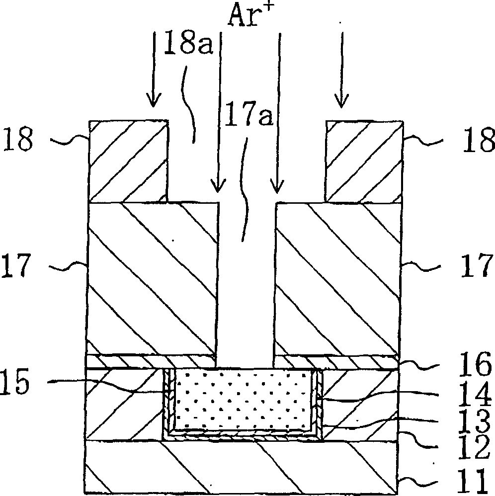
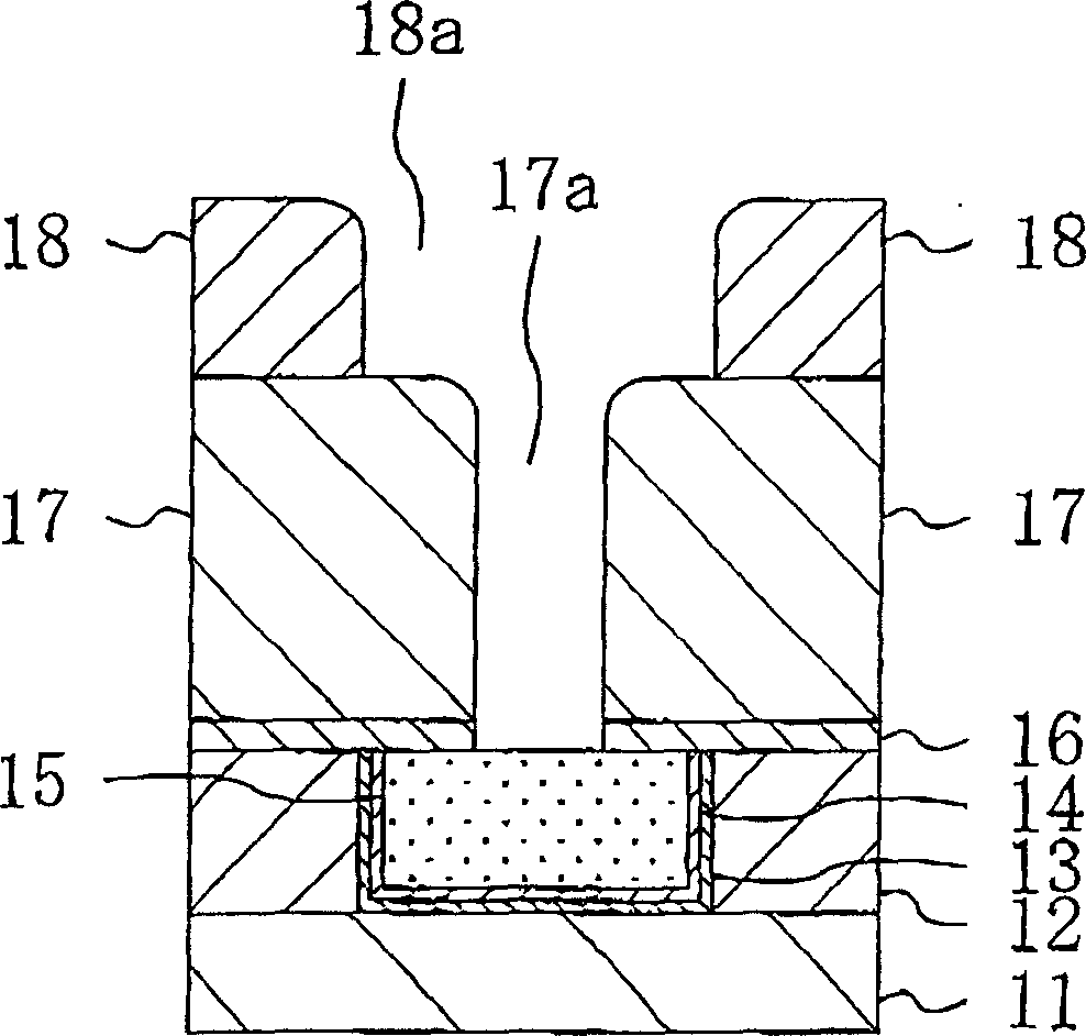
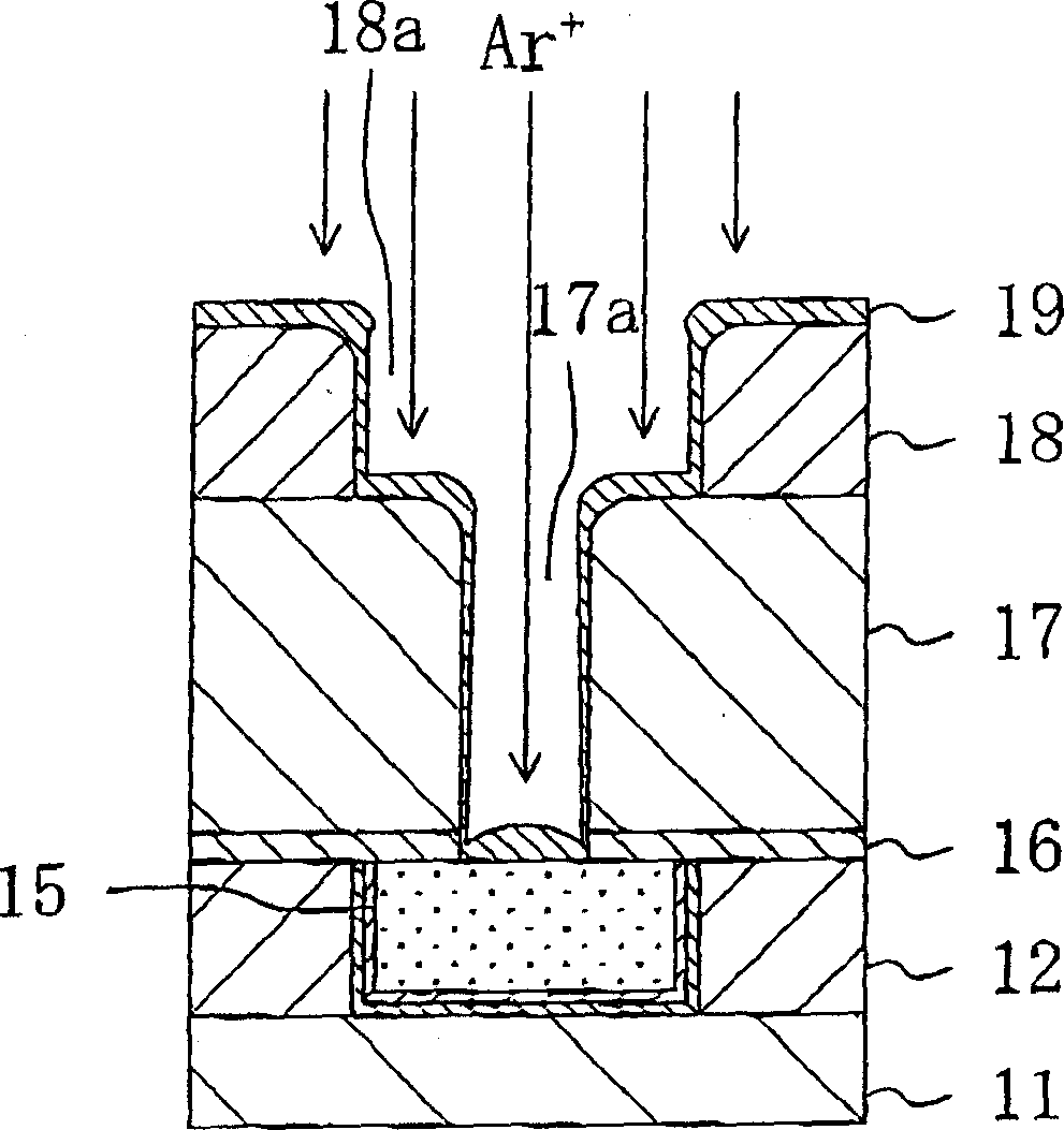
[0043] Figure 1(a), Figure 1(b) to Figure 6 (a), Image 6 (b) shows a cross-sectional structure of a part of the multilayer wiring including via holes (connection holes) shown in the order of processes in the method of manufacturing a semiconductor device according to an embodiment of the present invention.
[0044] First, as shown in FIG. 1(a), BPSG (Boron Phosphorous Silicate Glass) to form the first insulating film 11 and the second insulating film 12; use photolithography and dry etching to form the lower wiring to form grooves in a certain area of the second insulating film 12. Thereafter, the lower barrier layer 13 made of tantalum nitride (TaN) and the upper barrier layer made of tantalum (Ta) are deposited on the entire surface of the second insulating film 12 including the lower wiring formation groove by sputtering. 14. Next, a coating...
PUM
 Abstract
Description
Claims
Application Information
 - R&D
- Intellectual Property
- Life Sciences
- Materials
- Tech Scout
- Unparalleled Data Quality
- Higher Quality Content
- 60% Fewer Hallucinations
Browse by: Latest US Patents, China's latest patents, Technical Efficacy Thesaurus, Application Domain, Technology Topic, Popular Technical Reports.
© 2025 PatSnap. All rights reserved.Legal|Privacy policy|Modern Slavery Act Transparency Statement|Sitemap|About US| Contact US: help@patsnap.com