Film-forming material, lithographic film-forming composition, optical component-forming material, resist composition, resist pattern formation method, resist permanent film, radiation-sensitive composition, amorphous film production method, lithographic underlayer film-forming material, lithographic underlayer film-forming composition, lithographic underlayer film production method, and circuit pattern formation method
Composition and underlayer technology, applied to film forming material, film forming composition for lithography, material for forming optical parts, resist composition, resist pattern formation, permanent film for resist, radiation sensitive Composition, manufacture of amorphous film, material for forming an underlayer film for lithography, composition for forming an underlayer film for lithography, manufacture of an underlayer film for lithography, and circuit pattern formation, can solve the problem of resolution resist pattern collapse, difficult Get film thickness and other issues
- Summary
- Abstract
- Description
- Claims
- Application Information
AI Technical Summary
Problems solved by technology
Method used
Image
Examples
Embodiment 1
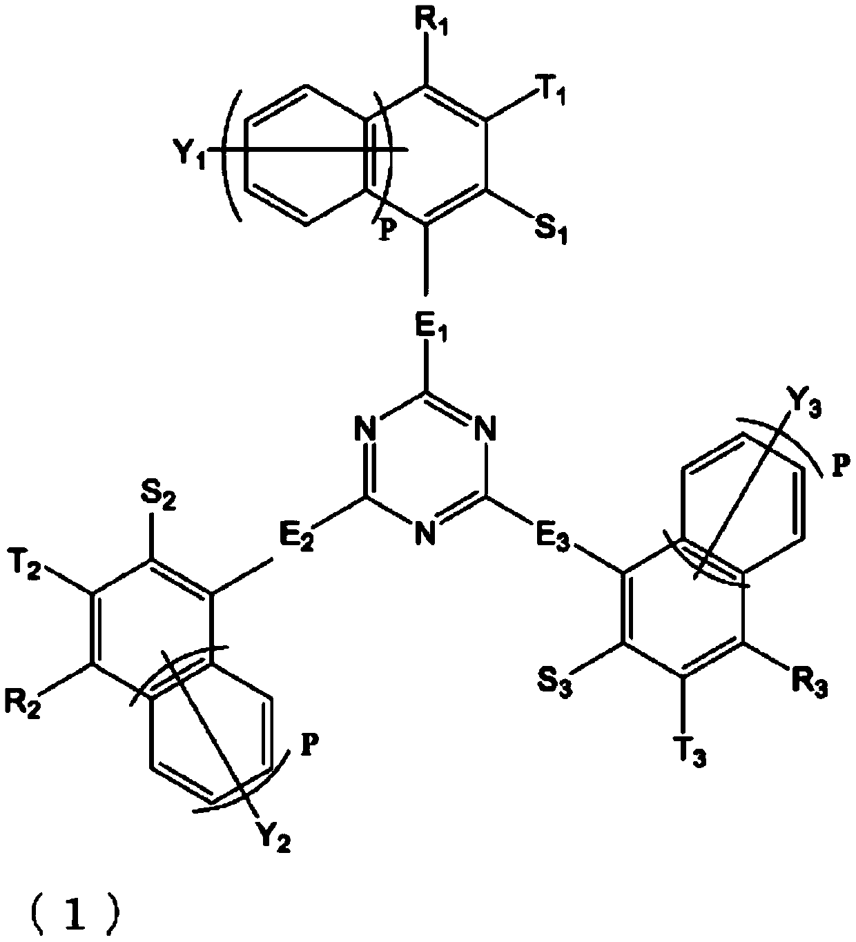
[0408] A triazine compound (LA-F70 manufactured by ADEKA Corporation) having a structure represented by the following formula was used alone as a material for forming a film for lithography.
[0409]
[0410] As a result of thermogravimetric measurement, the amount of heat loss at 400° C. of the obtained material for forming a photoresist film was less than 10% (evaluation A). In addition, as a result of evaluating the solubility to OX, it was 10% by mass to less than 15% by mass (evaluation B), and it was evaluated that the obtained material for forming a photoresist film had sufficient solubility.
[0411] 90 parts by mass of OX was added as a solvent to 10 parts by mass of the above-mentioned photoresist film-forming material, and stirred with a stirrer at room temperature for at least 3 hours, thereby producing a film-forming composition for lithography.
Embodiment 2
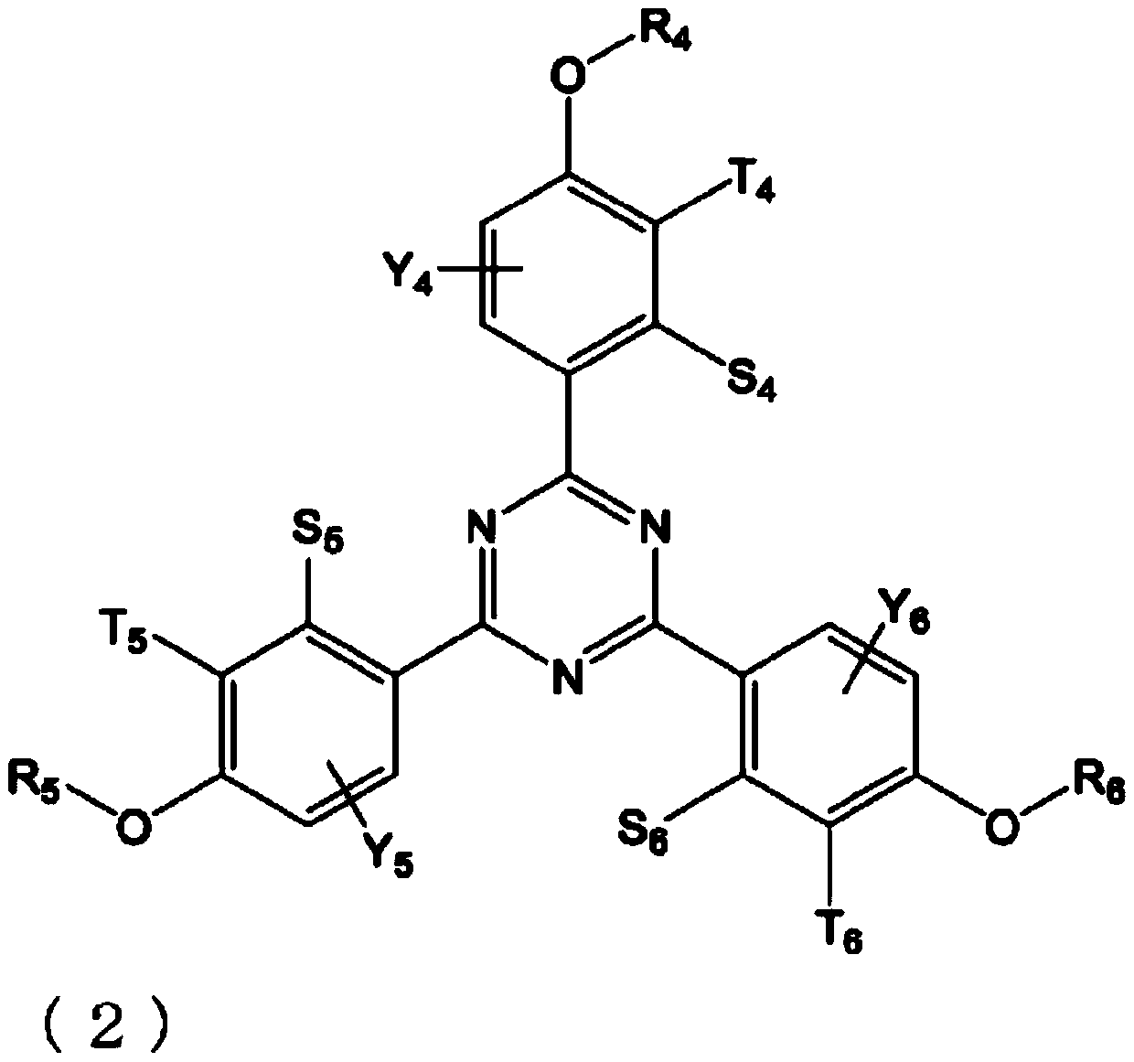
[0413] As a material for forming a film for lithography, a triazine compound (TINUVIN460 manufactured by BASF Corporation) having a structure represented by the following formula was used alone.
[0414]
[0415]As a result of the thermogravimetric measurement, the amount of heat loss at 400° C. of the obtained material for forming a photoresist film was 10% to 25% (evaluation B). Moreover, as a result of evaluating the solubility to OX, it was 15% by mass or more (evaluation A), and it was evaluated that the obtained material for forming a photoresist film had excellent solubility.
[0416] 90 parts by mass of OX was added as a solvent to 10 parts by mass of the above-mentioned photoresist film-forming material, and stirred with a stirrer at room temperature for at least 3 hours, thereby producing a film-forming composition for lithography.
Embodiment 3~5、 comparative example 2
[0433] (Manufacture of resist composition)
[0434] Using the above-mentioned film-forming materials, a resist composition was prepared by compounding as shown in Table 2. In addition, among the components of the resist composition in Table 2, the acid generator (C), the acid diffusion control agent (E) and the solvent used the following.
[0435] Acid generator (C): P-1: Triphenylsulfonium triflate (Midori Kagaku Co., Ltd)
[0436] Acid diffusion control agent (E): Q-1: Trioctylamine (Tokyo Chemical Industry Co., Ltd.)
[0437] Solvent: S-1: Propylene glycol monomethyl ether (Tokyo Chemical Industry Co., Ltd.)
[0438] (Evaluation Method of Resist Performance of Resist Composition)
[0439] After the uniform resist composition was spin-coated on a clean silicon wafer, pre-exposure baking (PB) was performed in an oven at 110° C. to form a resist film with a thickness of 60 nm. The obtained resist film was irradiated with electron beams set at 1:1 line and space (line and s...
PUM
| Property | Measurement | Unit |
|---|---|---|
| glass transition temperature | aaaaa | aaaaa |
Abstract
Description
Claims
Application Information
 - R&D
- Intellectual Property
- Life Sciences
- Materials
- Tech Scout
- Unparalleled Data Quality
- Higher Quality Content
- 60% Fewer Hallucinations
Browse by: Latest US Patents, China's latest patents, Technical Efficacy Thesaurus, Application Domain, Technology Topic, Popular Technical Reports.
© 2025 PatSnap. All rights reserved.Legal|Privacy policy|Modern Slavery Act Transparency Statement|Sitemap|About US| Contact US: help@patsnap.com


