Filming method of substrate and filming appts.
A coating device and substrate technology, applied to electrical components, cells, electrolytic processes, etc., can solve problems such as reduced reliability, poor graphics, and deterioration of electromigration resistance
- Summary
- Abstract
- Description
- Claims
- Application Information
AI Technical Summary
Problems solved by technology
Method used
Image

Examples
no. 1 Embodiment approach
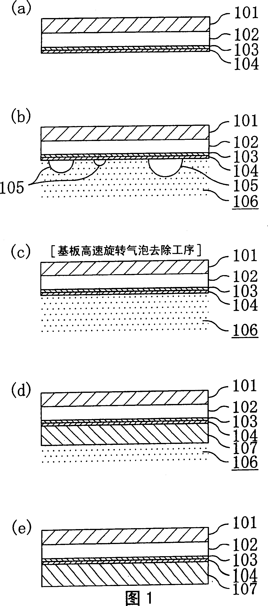
[0038] Hereinafter, a substrate coating method according to a first embodiment of the present invention will be described with reference to the drawings.
[0039] 1( a ) to ( e ) are cross-sectional views showing each step in the substrate coating method of the first embodiment. In addition, in FIG.1(a)-(e), the main surface of the board|substrate on which wiring etc. are formed is shown in the state facing down.
[0040] First, as shown in FIG. 1( a ), an interlayer insulating film 102 , a TaN barrier film 103 , and a Cu seed film 104 are sequentially deposited on a substrate 101 .
[0041] Then, as shown in FIG. 1( b ), the substrate 101 is clamped by a substrate clamping mechanism (not shown), and at the same time, the substrate 101 is immersed in the plating solution 106 face down by the mechanism. At this time, air bubbles 105 are adsorbed on the surface of the Cu seed film 104 on the surface to be plated. Here, the bubbles 105 are minute bubbles with a size of several ...
no. 2 Embodiment approach
[0059] Next, a substrate coating method according to a second embodiment of the present invention will be described with reference to the drawings.
[0060] Figure 4 (a) to (e) are sectional views showing each step in the substrate coating method according to the second embodiment of the present invention. Moreover, in Figure 4 In (a)-(e), the main surface of the board|substrate on which wiring etc. are formed is shown with the front facing down.
[0061] First, if Figure 4 As shown in (a), an interlayer insulating film 102 , a TaN barrier film 103 , and a Cu seed film 104 are sequentially deposited on a substrate 101 .
[0062] Then, in the present embodiment, while the substrate 101 is clamped by the substrate clamping mechanism (not shown) in a state facing downward, pure water is sprayed from the pure water nozzle 111 to the surface of the Cu seed film 104 on the surface to be plated. Stream 112.
[0063] However, as in the usual coating process, after the depositi...
no. 3 Embodiment approach
[0079] Next, a substrate coating method according to a third embodiment of the present invention will be described with reference to the drawings.
[0080] Figure 5 (a) to (e) are sectional views showing each step of the substrate coating method according to the third embodiment of the present invention. Moreover, in Figure 5 In (a)-(e), the main surface of the board|substrate on which wiring etc. are formed is shown with the front facing down.
[0081] First, if Figure 5 As shown in (a), an interlayer insulating film 102 , a TaN barrier film 103 , and a Cu seed film 104 are sequentially deposited on a substrate 101 . At this time, fine particles 115 of copper or the like generated during deposition of the Cu seed film 104 adhere to the surface of the Cu seed film 104 . When the substrate 101 is immersed in the plating solution with the particles 115 present on the surface of the Cu seed film 104 , bubbles with the particles 115 as nuclei are generated, resulting in def...
PUM
| Property | Measurement | Unit |
|---|---|---|
| size | aaaaa | aaaaa |
| diameter | aaaaa | aaaaa |
| thickness | aaaaa | aaaaa |
Abstract
Description
Claims
Application Information
 - R&D
- Intellectual Property
- Life Sciences
- Materials
- Tech Scout
- Unparalleled Data Quality
- Higher Quality Content
- 60% Fewer Hallucinations
Browse by: Latest US Patents, China's latest patents, Technical Efficacy Thesaurus, Application Domain, Technology Topic, Popular Technical Reports.
© 2025 PatSnap. All rights reserved.Legal|Privacy policy|Modern Slavery Act Transparency Statement|Sitemap|About US| Contact US: help@patsnap.com