
Low-power consumption related bi-sampling circuit structure
A technology of correlated double sampling and circuit structure, applied in the field of microelectronics, can solve the problems of many transistors, increased power consumption, low power consumption design without optimized readout circuit, etc.
- Summary
- Abstract
- Description
- Claims
- Application Information
AI Technical Summary
Problems solved by technology
Method used
Image



Examples
Embodiment Construction
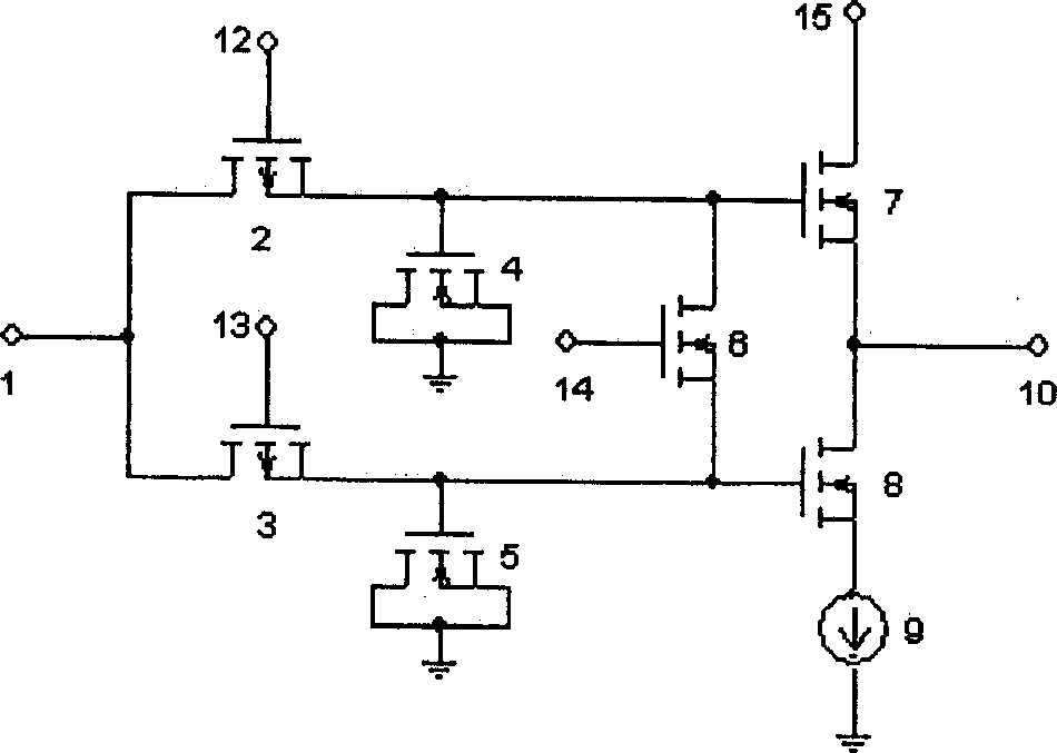
[0012] refer to figure 1 as shown, figure 1 It is the structure diagram of the first embodiment of the low power consumption correlated double sampling circuit structure of the present invention. The present invention is a low power consumption correlated double sampling circuit structure, which has the advantages of low power consumption and simple circuit structure, including:
[0013] Two P-type MOS tubes 2 and 3 for switching, the drains of P-type MOS tubes 2 and 3 for switching are connected to the signal input terminal 1, the gate of P-type MOS tube 2 for switching is connected to the set switch signal 12, and the P-type MOS tubes for switching are connected to the signal input terminal 1. The gate of the N-type MOS tube 3 is connected to the sampling switch signal 13; the capacitor uses N-type MOS tubes 4 and 5, and the drains and sources of the N-type MOS tubes 4 and 5 are grounded for the capacitor, and the N-type MOS tube 4 is used for the capacitor. The gate is con...
PUM
 Abstract
Description
Claims
Application Information