Optical module and its manufacturing method

A technology of an optical module and a manufacturing method, which is applied in the field of optical modules and can solve the problems of difficult and economical taper part processing and the like

Inactive Publication Date: 2004-05-12
NIPPON TELEGRAPH & TELEPHONE CORP
View PDF0 Cites 35 Cited by
  • Summary
  • Abstract
  • Description
  • Claims
  • Application Information

AI Technical Summary

Problems solved by technology

Therefore, it is difficult to treat the tapered part economically

Method used


Image

  • Optical module and its manufacturing method
  • Optical module and its manufacturing method
  • Optical module and its manufacturing method

Examples


no. 1 example

[0055] Figures 3A to 3C An optical module according to a first embodiment of the present invention is shown. refer to Figures 3A to 3C , reference numeral 20 denotes a first optical waveguide made of silicon like an electric wire; 21 denotes a mode field size conversion portion; 22 denotes a second optical waveguide connected to the first optical waveguide 20; 23 denotes a silicon substrate; 24 denotes a A lower cladding layer formed of a silicon dioxide film and provided over a silicon substrate 23; 25 denotes an upper cladding layer made of a polymer; 26 denotes a cladding layer made of silicon and forming the first optical waveguide 20 27 represents a tapered portion made of the same silicon as the first core 26, wherein, in accordance with its width dimension, decreases toward its end, while the height (thickness) of the cross-section of the core 26 remains 28 represents the second core that is made of polymer and is the core of the mode field size conversion portion 2...

no. 2 example

[0075] Figures 7A to 7C An optical module according to a second embodiment of the present invention is shown. exist Figures 7A to 7C in, with Figures 3A to 3C Like reference numerals denote like parts. The present embodiment is characterized in that silicon dioxide film 30 is formed only adjacent to the side surface of tapered portion 27 . This enables the tapered portion 27 to be shaped with high precision.

[0076] The following will refer to Figures 8A to 8G to describe Figures 7A to 7C The fabrication method of the optical module is shown.

[0077] exist Figures 8A to 8D The steps in are the same as those in the first embodiment Figures 4A to 4D The steps are the same as in . In the first embodiment, by using the mask 29 to etch the silicon layer 31, the first core 26 of the first optical waveguide 20 and the tapered portion 27 continuous with the core 26 are formed, and the mask 29 is removed. After that, an oxidation process is performed. In this embodi...

no. 3 example

[0086] This example is for Figures 4A to 4H The improvement of the manufacturing method of the optical module is shown, and only a part of the method is exemplified, wherein, in particular, after the silicon layer serving as the first core is formed on the lower cladding layer, a silicon dioxide film is formed to cover the first fiber core. Using this embodiment, optical modules can be manufactured in a shorter manufacturing time period than conventional methods.

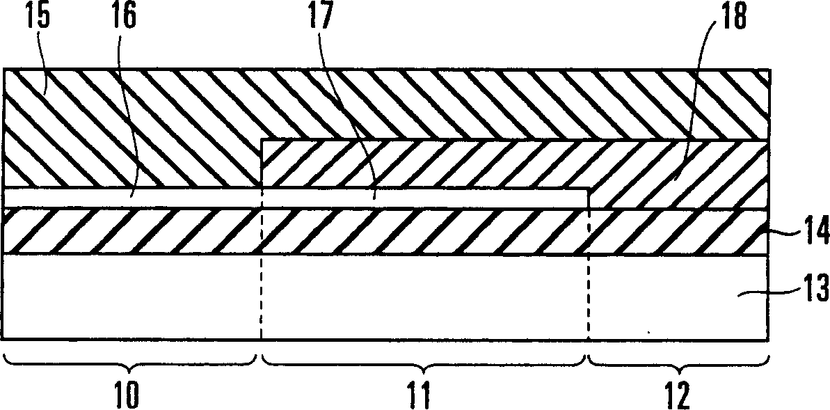
[0087] refer to Figures 9A to 9C , reference numeral 111 represents a silicon substrate; 112 represents a silicon dioxide film (SiO 2 ) formed under cladding; and, 113 denotes the core serving both as the first core and the tapered portion of the first optical waveguide in the above-described first embodiment. The core 113 is made of silicon, and forms a pattern of thin electric wires. Reference numeral 114 denotes a silica film provided to cover the core 113 . In this case, the width and thickness of the core ...


PUM


Abstract

A mode-field transforming planar optical waveguide device includes an under cladding, a first core, a second core, and an over cladding. The under cladding has a flat shape as a whole. The first core has a quadrangular cross section and is placed on the under cladding. The second core is placed on a tapered end portion of the first core. The over cladding is placed in a region including the tapered end portion of the first core and the second core. The under cladding and the first core placed thereon constitute a first optical waveguide. The under cladding, the tapered end portion of the first core placed on the under cladding, the second core placed thereon, and the over cladding placed on and around the second core constitute a mode field size conversion portion. The under cladding, the second core, and the over cladding constitute a second optical waveguide. The first core is made of silicon. The first and second cores differ in cross-sectional shape. A manufacturing method for the optical module is also disclosed.

Description

technical field [0001] The invention relates to an optical module used in the fields of optoelectronics and optical communication, and a manufacturing method of the optical communication module. Background technique [0002] Recently, various studies and developments have been conducted on silicon wire optical waveguides and photonic crystal waveguides using SOI (Silicon On Insulator) substrates for the purpose of downsizing optical circuits. According to the size (diameter) of the respective mode fields, problems arise in connection between these optical waveguides and optical fibers, light emitting devices, light receiving devices, and the like. These optical waveguides have mode field sizes on the submicron order, whereas optical fibers and the like have mode field sizes on the order of several microns. Therefore, it is difficult to efficiently establish a direct connection between an optical waveguide and a general-purpose optical fiber or the like having a large mode f...

Claims


Application Information

Patent Timeline
Patent Type & Authority Applications(China)
IPC IPC(8): G02B6/12G02B6/122G02B6/30
CPCG02B2006/12176G02B6/305G02B6/1228
Inventor 山田浩治土泽泰内山真吾壮司哲史高桥淳一渡边俊文为近惠美森田博文
Owner NIPPON TELEGRAPH & TELEPHONE CORP
Why Eureka
Try Eureka