Fuse wire possessing cover layer and forming method

A covering layer and fuse technology, which is applied in electrical components, semiconductor/solid-state device manufacturing, circuits, etc., can solve problems such as difficulty in controlling the etched depth of the fuse window 107b, failure of the fuse 107b to be pierced, and loss of function.

Inactive Publication Date: 2004-05-26
TAIWAN SEMICON MFG CO LTD
View PDF1 Cites 3 Cited by
  • Summary
  • Abstract
  • Description
  • Claims
  • Application Information

AI Technical Summary

Problems solved by technology

[0016] Because the thickness of the dielectric layer 109b at the position above the fuse 107b is relatively thin, it is easy to be etched through in the subsequent manufacturing process and lose its function; on the contrary, if the fuse window formed at the position above the fuse 107b has a shallow depth, to avoid If the dielectric layer is accidentally etched through, because the etched depth of the fuse window 107b above the fuse 107b is difficult to control, the dielectric layer above the fuse 107b may be made too thick. When repairing, the fuse 107b may not be punctured

Method used


Image

  • Fuse wire possessing cover layer and forming method
  • Fuse wire possessing cover layer and forming method
  • Fuse wire possessing cover layer and forming method

Examples


Embodiment Construction

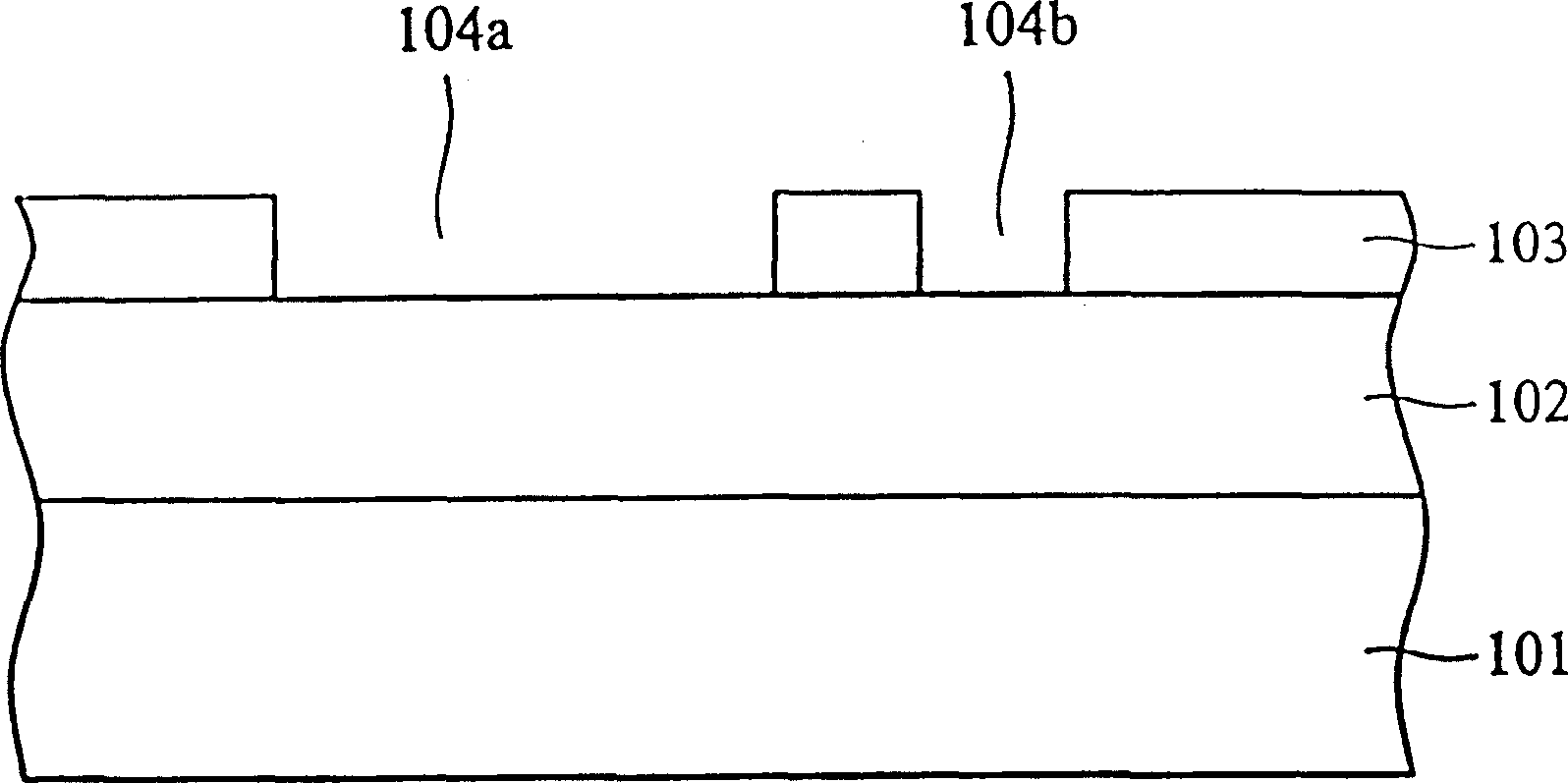
[0048] Please refer to Figure 2a Firstly, a semiconductor substrate 201 is provided, and any required elements can be formed on the semiconductor substrate 201 . A dielectric layer 202 and a patterned mask layer 203 are sequentially formed on the semiconductor substrate 201, the patterned mask layer 203 has openings 204a and 204b, the openings 204a and 204b will expose part of the surface of the dielectric layer 202, and The position of the opening 204a is the position of the subsequent formation of the metal interconnection, and the position of the opening 204b is the position of the subsequent formation of the fuse. Wherein, the semiconductor substrate 201 is, for example, silicon crystal; the dielectric layer 202 is, for example, a silicon oxide layer.

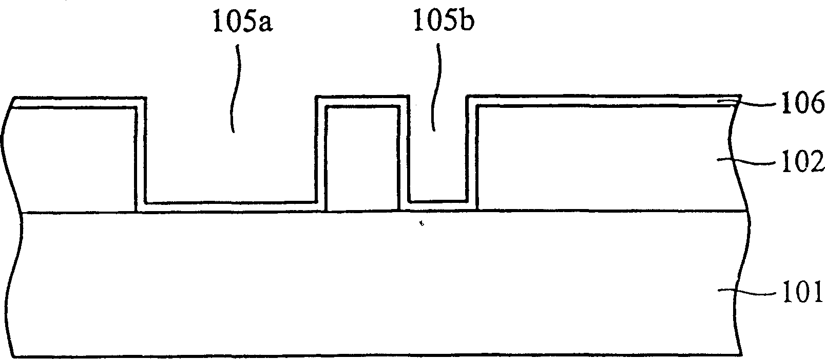
[0049] Please refer to Figure 2b , using the patterned mask layer 203 as a mask to etch the dielectric layer 202 to form openings 205 a and 205 b on the dielectric layer 202 , the openings 205 a and 205 b will expose pa...


PUM


Abstract

First, a substrate possessing intraconnection wire and structure of fuse wire is provided. Covering layer composed of first dielectric layer, stopping layer and second dielectric layer is formed on the substrate. First opening exposing surface of the intraconnection wire is formed on the covering layer, and metal welding pads higher than surface of covering layer is also formed on the first opening. Protective layer, antireflection layer and patterned mask layer possessing second and third openings are formed on the metal welding pads and the covering layer. The second opening exposes antireflection layer on the metal welding pads, the third opening exposes antireflection layer on fuse wire. Then, by using patterned mask layer, etching antireflection layer and protective layer in sequence along second opening as well as etching protective layer, second dielectric layer and stopping layer in sequence along third opening forms the fuse wire window.

Description

technical field [0001] The invention relates to a fuse and its forming method, in particular to a fuse with a covering layer and its forming method, which is suitable for semiconductor devices. The present invention is mainly to form a composite layer of oxide layer-stop layer-oxidation layer above the fuse, and retain an appropriate thickness of oxide layer with the help of the stop layer, so as to prevent excessive etching during the formation of the fuse window and expose the fuse or Damage the fuse, and avoid the chance that the fuse window may not be punctured if it needs to be repaired later. Background technique [0002] At present, after semiconductor devices enter the very large integrated circuit manufacturing process, the line spacing must be shortened to increase the density. In this way, the defects or defects generated in the manufacturing process tend to increase, and the output yield rate naturally decreases. Therefore, Integrated circuits (ICs) such as stat...

Claims


Application Information

Patent Timeline
IPC IPC(8): H01L21/70
Inventor 吴瑞国吴义郎吴林峻陈殿豪
Owner TAIWAN SEMICON MFG CO LTD
Why Eureka
Try Eureka