

Semiconductor device, electronic appts. their mfg. methods and electronic instrument
A semiconductor and device technology, applied in the field of semiconductor devices, can solve the problems of difficulty in stacking different types of components, difficulty in stacking different types of chips, and inability to improve the effectiveness of space saving.
- Summary
- Abstract
- Description
- Claims
- Application Information
AI Technical Summary
Problems solved by technology
Method used
Image

Examples
Embodiment Construction
[0049] Semiconductor devices, electronic equipment and their manufacturing methods according to embodiments of the present invention will be described below with reference to the drawings.
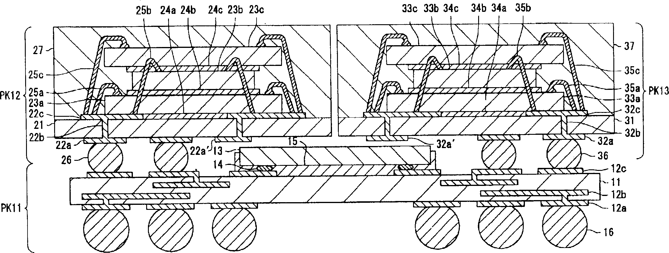
[0050] figure 1 is a cross-sectional view showing the structure of the semiconductor device of the first embodiment. In this first embodiment, on the semiconductor package PK11 on which the semiconductor chip (or semiconductor die) 13 is mounted by ACF bonding, the semiconductor package PK12 and the wire bonded semiconductor chip (or semiconductor die) 23a to 23c of the stacked structure are laminated respectively. The semiconductor package PK13 of the stacked semiconductor chips (or semiconductor dies) 33a to 33c is connected by soldering.
[0051] figure 1 In this example, a carrier substrate 11 is provided on the semiconductor package PK11, and connection platforms 12a and 12c are respectively formed on both sides of the carrier substrate 11, and internal wiring 12b is formed in the c...
PUM
 Abstract
Description
Claims
Application Information