Semiconductor device, electronic appts. their mfg. methods and electronic instrument

A manufacturing method and semiconductor technology, which are applied in the fields of semiconductor/solid-state device manufacturing, semiconductor devices, and semiconductor/solid-state device components, etc., can solve the problem of low space saving effectiveness

Inactive Publication Date: 2004-08-11
SEIKO EPSON CORP
View PDF1 Cites 8 Cited by
  • Summary
  • Abstract
  • Description
  • Claims
  • Application Information

AI Technical Summary

Problems solved by technology

[0003] However, in the method of three-dimensionally mounting semiconductor chips while inserting the same type of carrier substrate, it is difficult to stack different types of modules, and because of the difficulty of stacking different types of modules, there is a problem that the effectiveness of space saving is not high.

Method used


Image

  • Semiconductor device, electronic appts. their mfg. methods and electronic instrument
  • Semiconductor device, electronic appts. their mfg. methods and electronic instrument
  • Semiconductor device, electronic appts. their mfg. methods and electronic instrument

Examples


Embodiment Construction

[0051] A semiconductor device, an electronic device, and a manufacturing method thereof according to an embodiment of the present invention will be described below with reference to the drawings.

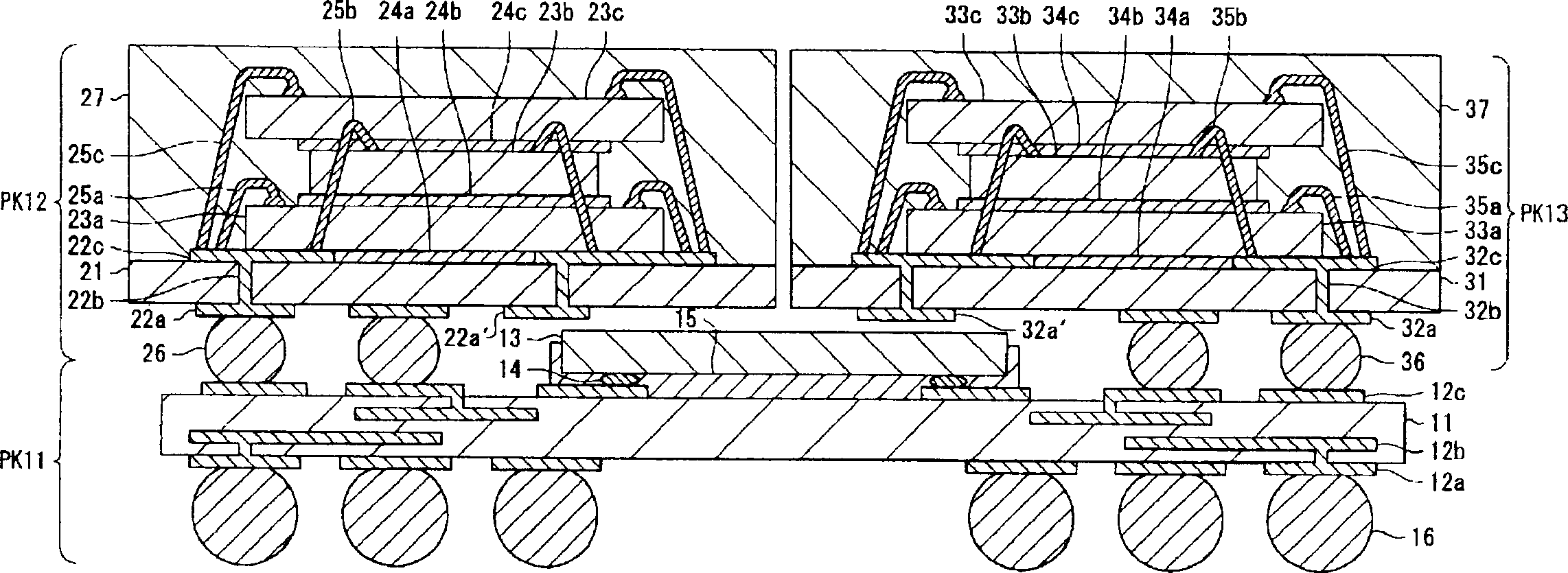
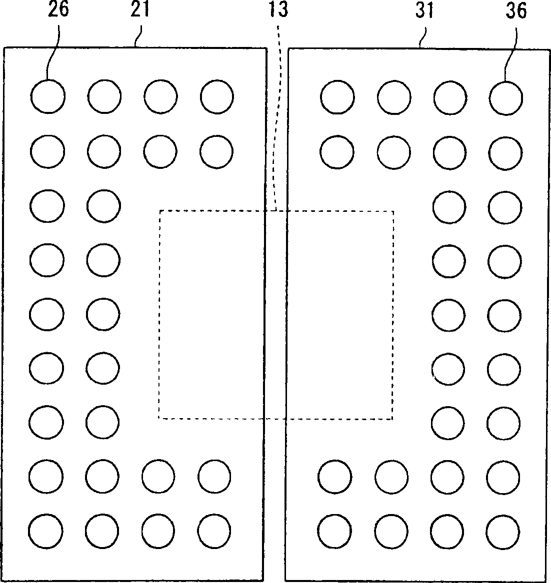
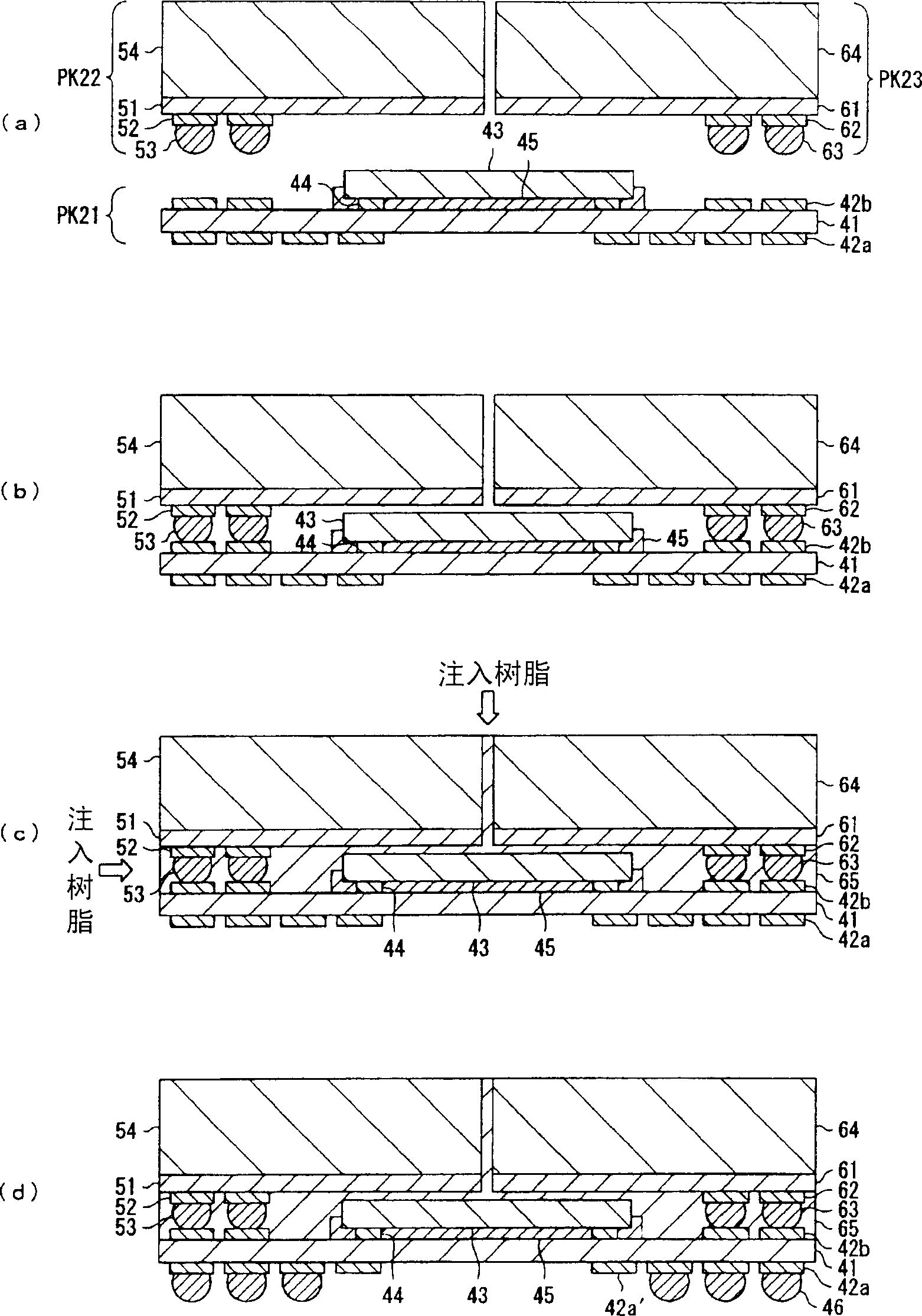
[0052] figure 1 is a cross-sectional view showing the structure of the semiconductor device of the first embodiment of the present invention, figure 2 It is a plan view showing a schematic structure of the semiconductor device of the first embodiment of the present invention. Also, in the first embodiment, on the semiconductor package PK11 in which the semiconductor chips (or semiconductor dies) are mounted by ACF bonding, the semiconductor packages PK12 in which the semiconductor chips (or semiconductor dies) 23a to 23c of the stacked structure are connected by wire bonding are laminated respectively. The semiconductor package PK13 of the stacked semiconductor chips (or semiconductor dies) 33a to 33c is connected by wire bonding.

[0053] figure 1 Among them, a carrier substrat...


PUM


Abstract

A method is provided to realize a three-dimensional mounting structure of different types of packages. By bonding protruding electrodes onto lands, which are formed on a first carrier substrate, second and third carrier substrates are mounted on the first carrier substrate such that ends of the second and third carrier substrates are arranged above a semiconductor chip.

Description

field of invention [0001] The present invention relates to a semiconductor device, an electronic device, an electronic instrument, a method for manufacturing the semiconductor device, and a method for manufacturing the electronic device. It is especially suitable for lamination structures of semiconductor components and the like. Background technique [0002] In existing semiconductor devices, in order to save space when semiconductor chips are mounted, there is a method of three-dimensionally mounting semiconductor chips while inserting the same type of carrier substrate as shown in Japanese Patent Application Laid-Open No. 10-284683, for example. [0003] However, in the method of three-dimensionally mounting semiconductor chips while inserting the same type of carrier substrate, it is difficult to stack different types of modules, and because of the difficulty in stacking different types of modules, there is a problem that the effectiveness of space saving is not high. ...

Claims


Application Information

Patent Timeline
Patent Type & Authority Applications(China)
IPC IPC(8): H01L25/18H01L21/56H01L23/31H01L23/48H01L23/52H01L23/538H01L25/065H01L25/07H01L25/10H01L25/11
CPCH01L2225/1058H01L2224/73203H01L2224/45124H01L23/3114H01L23/5385H01L2924/3511H01L2225/1005H01L2224/16H01L2224/73215H01L2224/73253H01L2225/1023H01L2924/15311H01L2924/01029H01L2924/15151H01L25/0652H01L2924/01013H01L2224/32225H01L2224/48225H01L2924/15331H01L21/56H01L2225/06568H01L24/48H01L2224/73204H01L2924/01079H01L2224/48465H01L25/105H01L25/0657H01L2224/48227H01L2224/32145H01L25/03H01L23/481H01L2224/45144H01L2224/16225H01L2224/73265H01L2225/06562H01L2924/00014H01L24/45H01L24/73H01L2924/181H01L2924/00012H01L2924/00H01L2224/05599H01L2224/0401
Inventor 泽本俊宏中山浩久青栁哲理
Owner SEIKO EPSON CORP
Why Eureka
Try Eureka