Light shield for contacting window making process and making process thereof

A technology of contact window and photomask, which is applied in the direction of original components, optics, and optomechanical equipment used for photomechanical processing, and can solve problems such as broken wires, poor coverage of pixel electrodes 110 steps, steepness, etc., and achieve the effect of increasing complexity

Inactive Publication Date: 2004-08-25
AU OPTRONICS CORP
View PDF0 Cites 0 Cited by
  • Summary
  • Abstract
  • Description
  • Claims
  • Application Information

AI Technical Summary

Problems solved by technology

However, due to the large thickness of the organic photosensitive material layer 104, the sidewalls of the contact opening 106 defined are too steep. In other words, the contact angle 108 between the sidewalls of the contact opening 106 and the underlying conductive layer 104 will be close to 70 degrees
[0005] Please refer to Figure 1B If the sidewall of the contact window opening 106 is too steep, it will cause poor step coverage of the pixel electrode 110 when the pixel electrode 110 is subsequently sputtered on the organic photosensitive material layer 104 and in the contact window opening 106, resulting in disconnection.

Method used


Image

  • Light shield for contacting window making process and making process thereof
  • Light shield for contacting window making process and making process thereof
  • Light shield for contacting window making process and making process thereof

Examples


Embodiment Construction

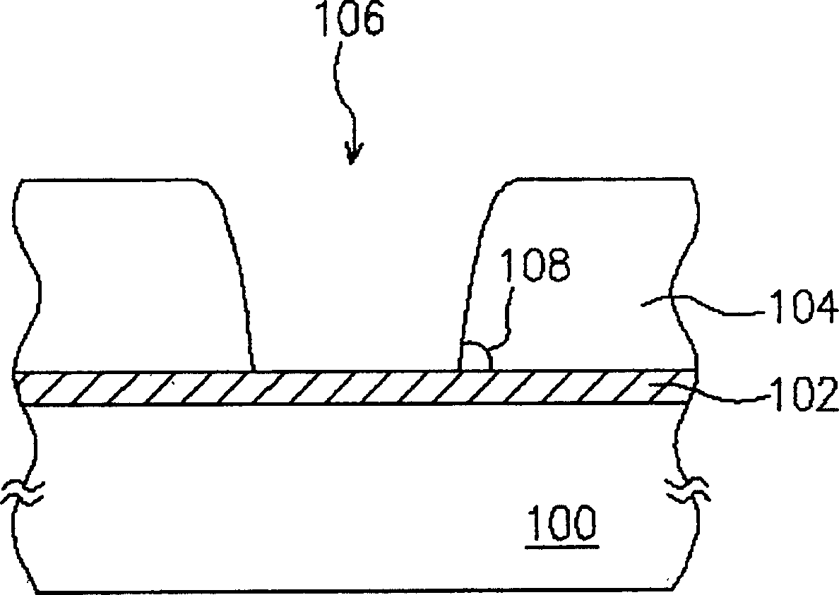
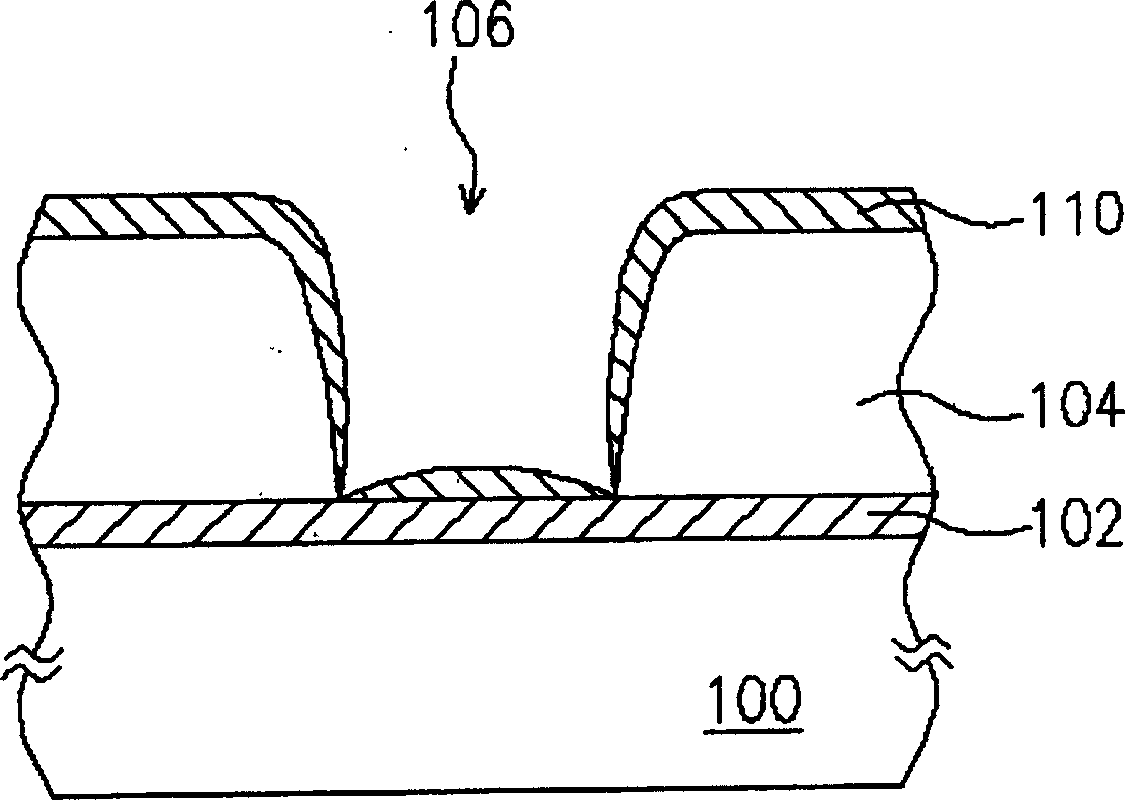
[0044] Such as Figure 2A to Figure 2E As shown, it shows a schematic cross-sectional view of the manufacturing process of the contact window according to a preferred embodiment of the present invention.

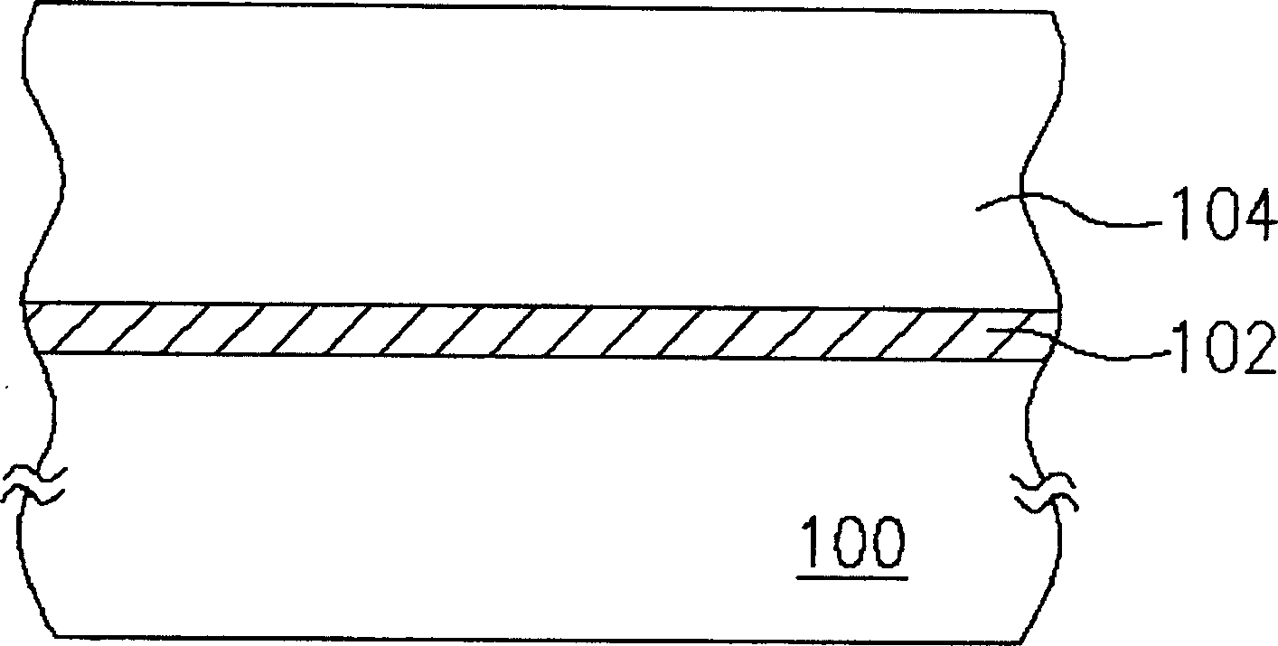
[0045] Please refer to Figure 2A , a substrate 100 is provided, a conductive layer 102 has been formed on the substrate 100 , and a dielectric layer 104 has been formed on the conductive layer 102 .

[0046] If the contact window process is applied in the liquid crystal display process, the conductive layer 102 is, for example, the second metal layer ( M2 ) in the TFT process, which can be the drain of the TFT or the upper electrode of the pixel storage capacitor. The dielectric layer 104 is, for example, a non-photosensitive inorganic dielectric material such as silicon nitride or silicon oxide, while in the manufacturing process of a liquid crystal display with a high aperture ratio, the dielectric layer 104 usually uses an organic photosensitive material (such as a phot...


PUM


Abstract

The invention is a k-portion fractal masking method for preparing material chip, according to maximum level number k of the elements in the material chip to be made, firstly separating the basic mask into k centrally symmetrical areas, namely k-portion fractal, one of the areas is set in a through state, rotating all the masks obtained at an angle of 360 degrees / k in the same direction, per rotation sputters a level of the first element, after the first period, there are k material units on the chip, after this, if a element is added every time, adopting a new mask, making the fractal on the masking areas corresponding to current material units on the chip according to the fractal mode of the basic mask, so as to obtain the next new mask, i.e. each mask has the structure similar to the basic mask, and then obtaining the material chip combined of any n elements whose maximum level number is k by n fractals and k rotation operations superposed.

Description

technical field [0001] The present invention relates to a photomask and its application, and in particular to a photomask applied in contact window process and its contact window process. Background technique [0002] In the manufacturing process of liquid crystal displays, non-photosensitive dielectric materials or organic photosensitive materials are usually used as the insulating layer of the thin film transistor array. In order to electrically connect the conductive layers above and below the insulating layer, patterns are generally used. A contact window opening is formed in the insulating layer by a chemical process (such as a lithography process and an etching process or simply using a lithography process), so that the conductive layer above and below the insulating layer can be conducted. For example, the method for electrically connecting the pixel electrode in the pixel structure to the drain of the thin film transistor is to perform a patterning process before for...

Claims


Application Information

Patent Timeline
IPC IPC(8): G02F1/133G03F1/38G03F7/00G03F9/00
Inventor 张志清颜士益
Owner AU OPTRONICS CORP
Why Eureka
Try Eureka