Method for preparing slice type network resistor and slice type network resistor prepared by the same method

A technology of resistors and manufacturing methods, applied in the direction of resistors, non-adjustable metal resistors, impedance networks, etc., can solve problems such as product failure, difficulty in size and thickness, short circuit of terminal electrodes, etc.

Inactive Publication Date: 2004-09-01
GUANGDONG FENGHUA ADVANCED TECH HLDG
View PDF0 Cites 18 Cited by
  • Summary
  • Abstract
  • Description
  • Claims
  • Application Information

AI Technical Summary

Problems solved by technology

However, when the dimensions of chip network resistors are miniaturized and the depth of the grooves on both sides of the insulating substrate is reduced to a certain extent, the above method of applying side electrode paste is not applicable.
Because the amount and thickness of the slurry applied by the above two methods are difficult to control, the electrode slurry has a certain fluidity, and the groove depth of the insulating substrate is very smal

Method used


Image

  • Method for preparing slice type network resistor and slice type network resistor prepared by the same method
  • Method for preparing slice type network resistor and slice type network resistor prepared by the same method
  • Method for preparing slice type network resistor and slice type network resistor prepared by the same method

Examples


Embodiment Construction

[0048] The present invention will be described in detail below with reference to the accompanying drawings; this embodiment takes a chip network resistor with four resistive layers as an example, but the present invention is not limited to a chip network resistor with four resistive layers.

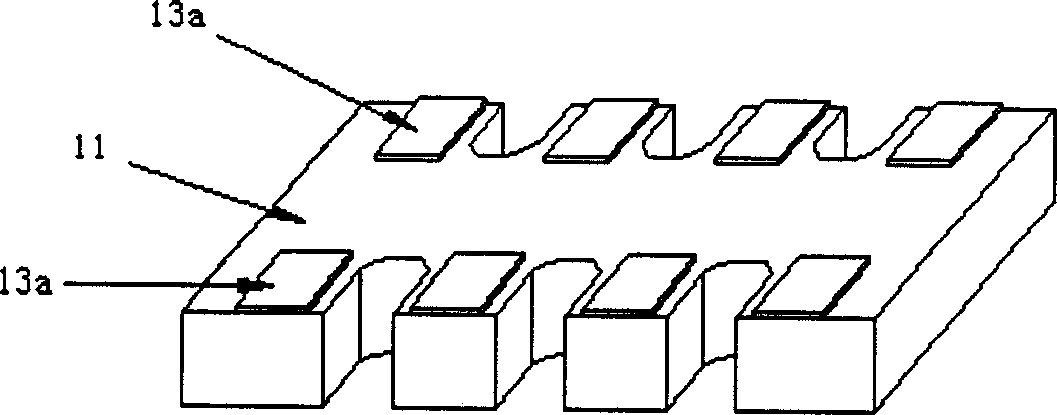
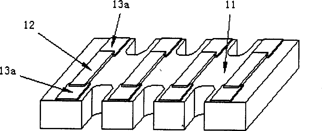
[0049] according to Figure 6 and Figure 7 The chip network resistor shown includes: an insulating substrate 11 made of alumina or ceramic or glass insulating material, four pairs of separated front electrodes 13a located on the protruding parts of the insulating substrate 11, four pairs of front electrodes 13a connected to the front surface The electrodes 13a are connected to the resistive layer 12 with each other.

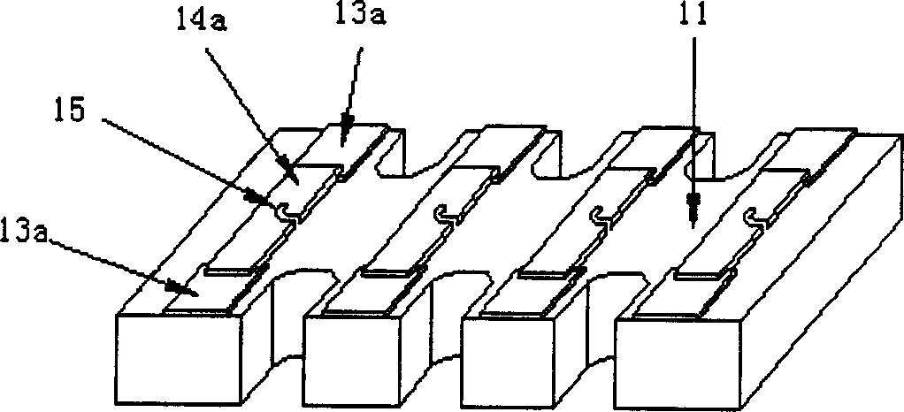
[0050] The resistive layer 12 is covered with a protective layer 14 . The protective layer 14 comprises an inner protective layer 14a of glass material directly overlying the resistive layer 12 and an outer protective layer 14b thereon. The resistance layer 12 and the in...


PUM


Abstract

The invention discloses a manufacturing method for a kind of piece network resistance and the product. The method includes following steps: (1) it forms two pairs or more separated front poles on the upper surface of the insulating base piece; (2) forms two or more resistance layers connected to each pair of front surface poles on the insulating base piece; (3) forms a protection layer on the resistance layer; (4) forms the side poles on the convex part on the side surface of the base piece. It uses subjacent coating mode to add pole pulp on the convex part of the side surface in step (4). The invention can avoid the short pass between the side poles; the piece network resistance has excellent performance.

Description

technical field [0001] The invention relates to a manufacturing method of a chip network resistor and the manufactured chip network resistor, in particular, the invention relates to a manufacturing method of a side electrode of a chip network resistor. Background technique [0002] A typical chip network resistor includes a rectangular insulating substrate, a plurality of resistance layers with the required resistance value formed on it, and a plurality of pairs of terminal electrodes connected to the resistance layer are formed at both ends of the resistance layer, and in order to protect the resistance layer and a protective layer covering the resistive layer is formed on it. [0003] A typical structure of the above-mentioned chip network resistor is as follows: Figure 8 As shown, it includes: an insulating substrate 1, a resistive layer 2 formed on the insulating substrate 1, terminal electrodes 3 (the terminal electrodes are located at the two ends of the resistive lay...

Claims


Application Information

Patent Timeline
IPC IPC(8): H01C7/00H01C17/06H03H1/00
Inventor 张俊杨晓平陈肇强李东朝莫雪琼王勇华
Owner GUANGDONG FENGHUA ADVANCED TECH HLDG
Why Eureka
Try Eureka