Non electrode plane medium blockage discharge fluorescent lamp and its making method
A dielectric barrier discharge and electrodeless technology, which is applied in the manufacture of discharge tubes/lamps, electrode system manufacturing, and parts of gas discharge lamps, can solve the problem of large-scale and large-scale flat light sources that have not been found in literature or reports. Industrialized production, damage to mechanical strength and surface flatness, etc., to achieve the effect of protecting mechanical strength and surface flatness, ensuring performance, and reducing production costs
- Summary
- Abstract
- Description
- Claims
- Application Information
AI Technical Summary
Problems solved by technology
Method used
Image
Examples
Embodiment 1
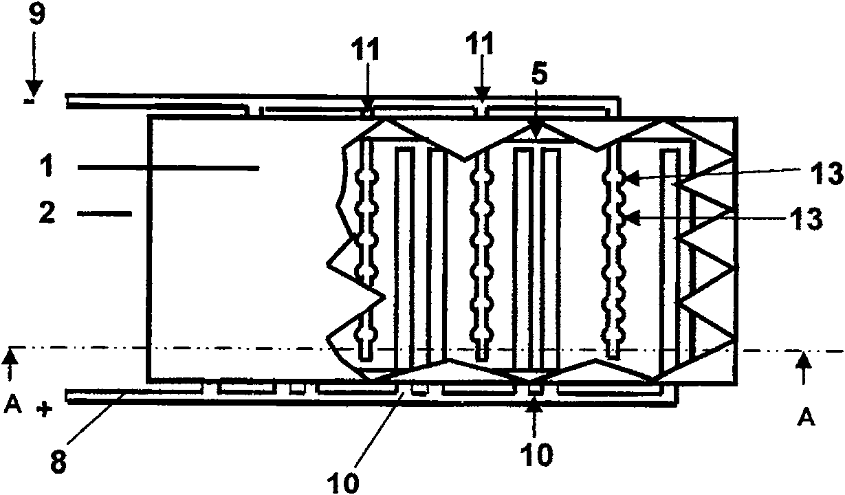
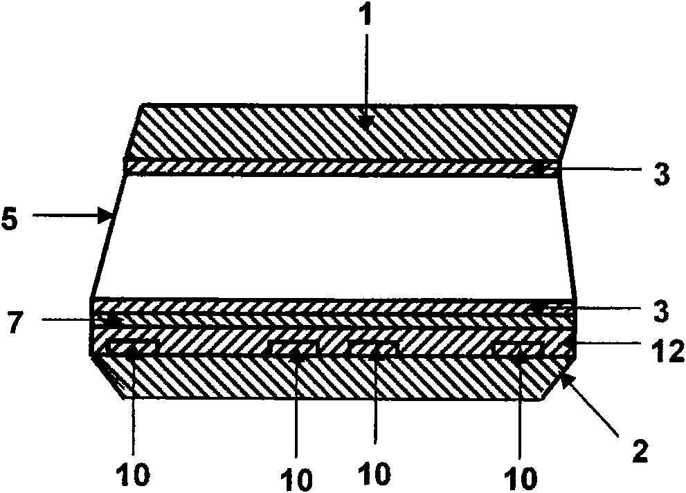
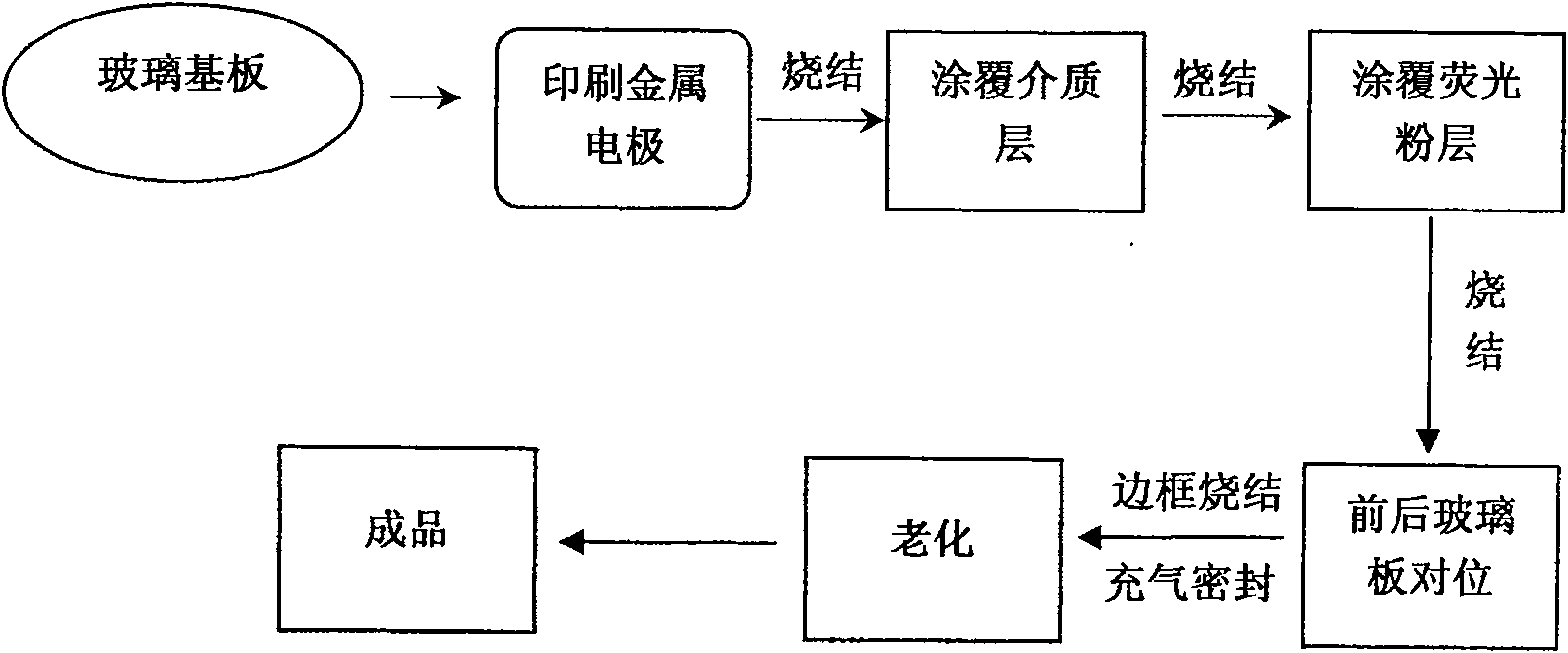
[0038] Referring to Fig. 3, the present invention is a non-polar planar dielectric barrier discharge fluorescent lamp, its appearance is shown in Fig. 3 (a), and its internal structure section structure is shown in Fig. 3 (b). The non-polar planar dielectric barrier discharge fluorescent lamp includes a front glass A certain distance is maintained between the substrate 1 and the rear glass substrate 2, and between the front glass substrate 1 and the rear glass substrate 2 through the barrier 4, and the barrier 4 adopts a curved shape, as shown in FIG. 5(b). They are sealed together with a low-melting-point glass frame 5 at the periphery. Phosphor powder layers 3 are arranged on the inner surfaces of the two glass plates, and the phosphor powder coating is obtained by screen printing, and then sintered to remove the binder to obtain the adsorption of the phosphor powder layer to the glass substrate. Barriers and frames are arranged on the rear glass substrate 2 as supports, and...
Embodiment 2
[0041] The overall structure is the same as that of Embodiment 1, except that phosphor layers 3 are arranged on the inner surfaces of the two glass substrates, and the phosphor coating is obtained by spraying. The barrier 4 adopts a linear shape, see FIG. 5( a ).
Embodiment 3
[0043] Overall structure is the same as embodiment 1 or embodiment 2, and transparent conductive medium layer 6 is formed conductive medium layer by sealing one deck transparent water film, and this conductive medium layer can pass a piece of ultra-thin glass plate on the outer surface of front and rear glass substrates, surround with UV curing glue is used to seal, forming a cavity with a certain thickness, and then injecting water from the reserved small hole. The method avoids the printing and sintering of precious metal electrodes, not only saves the production cost, but also reduces the damage to the glass substrate caused by sintering, and at the same time greatly simplifies the process.
PUM
 Abstract
Description
Claims
Application Information


