

Placode binder and binding method
A technology for bonding devices and substrates, used in optics, instruments, electrical components, etc., can solve the problems of uneven substrate spacing, difficulty in making stable products, and increased device weight, preventing uneven substrate spacing and reducing display. Poor phenomenon, the effect of keeping the parallelism uniform
- Summary
- Abstract
- Description
- Claims
- Application Information
AI Technical Summary
Problems solved by technology
Method used
Image

Examples
no. 1 example
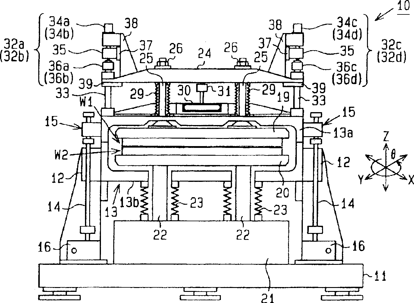
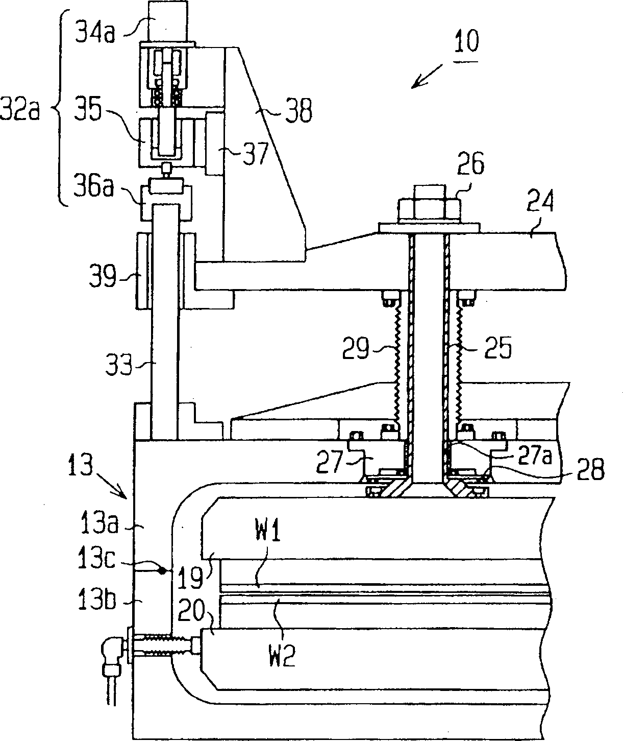
[0028] Below, according to Figure 1 to Figure 5 The first embodiment embodying the present invention will be described.
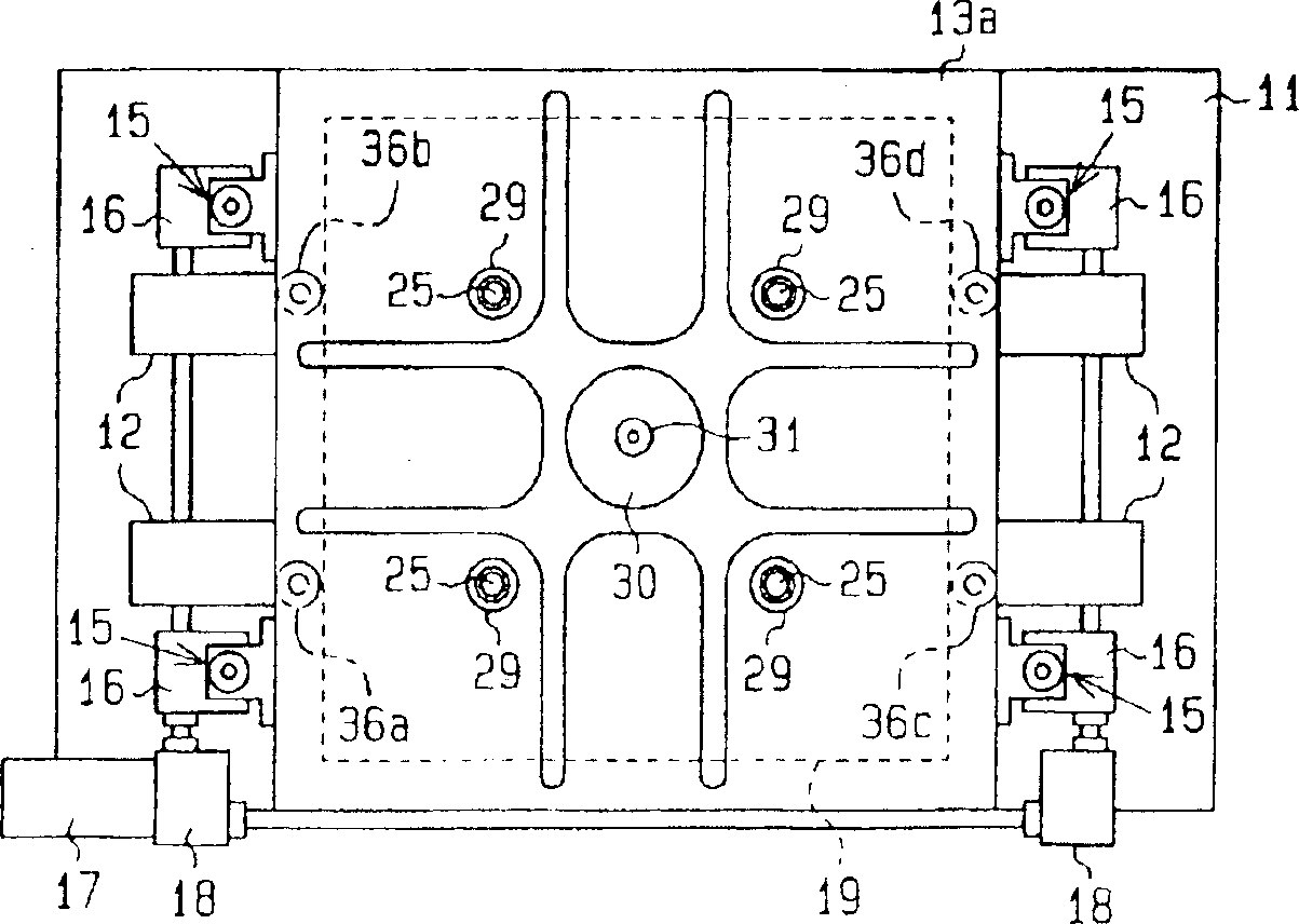
[0029] figure 1 It is a front view showing a schematic structure of a substrate bonding apparatus (hereinafter referred to as bonding apparatus) 10 of the first embodiment, figure 2 is a top view of the bonding device 10, image 3 It is a partially enlarged view of the bonding device 10 . This bonding apparatus 10 bonds two kinds of first and second substrates W1 and W2 supplied with liquid crystal dropwise in advance to one of them to form a liquid crystal display panel.
[0030] Moreover, the liquid crystal display panel produced by this embodiment is an active matrix type liquid crystal display panel, the first substrate W1 is a color filter substrate (CF substrate) on which a color filter or a light-shielding film is formed, and the second substrate W1 is a color filter substrate (CF substrate). W2 is an array substrate (TFT substrate) on which TF...
no. 2 example
[0077] Below, according to Image 6 and Figure 7 A second embodiment embodying the present invention will be described.
[0078] In addition, in the present embodiment, the same reference numerals are assigned to the parts having the same configuration as those in the above-mentioned first embodiment, and description thereof will be omitted.
[0079] Image 6 It is a side view showing a schematic structure of a substrate bonding device (hereinafter referred to as bonding device) 50 of the second embodiment, Figure 7 is along Image 6 A cross-sectional view of bonding apparatus 50 taken along line A-A is shown. Similar to the first embodiment, the bonding device 50 bonds the first and second substrates W1, W2 to form a liquid crystal display panel.
[0080] like Image 6 As shown, the bonding apparatus 50 includes an inner cavity 51, and a pressure plate 52 for absorbing and holding the first substrate W1 is provided in an upper container 51a of the inner cavity 51. Mo...
PUM
 Abstract
Description
Claims
Application Information