Method of ultrasonic-mounting electronic component and ultrasonic mounting machine

a technology of ultrasonic mounting and electronic components, which is applied in the direction of mechanical control devices, instruments, process and machine control, etc., can solve the problems of difficult to correctly apply energy to the bonding section, and the electronic component cannot be mounted with the prescribed bonding strength, so as to and improve the bonding section between the electronic component and the circuit board.

Inactive Publication Date: 2007-04-24
FUJITSU LTD
View PDF2 Cites 8 Cited by
  • Summary
  • Abstract
  • Description
  • Claims
  • Application Information

AI Technical Summary

Benefits of technology

[0014]An object of the present invention is to provide a method of ultrasonic-mounting an electronic component, which is capable of uniformly bonding bumps of the electronic component to a circuit board and improving reliability of ultrasonic-mounting the electronic component.
[0017]In the method, the loads may be maximized at first positions, at each of which displacement of the electronic component in the direction of the vibrations is zero, and the loads may be minimized at second positions, at each of which displacement of the electronic component in the direction of the vibrations is maximum. With this method, bondability of bonding sections between the electronic component and the circuit board can be improved, so that the both can be securely flip-chip-bonded. Note that, the effect can be sufficiently gained when the displacement of the electronic component is not only zero and the maximum but also near zero and near maximum.
[0018]In the method, the loads may be periodic-functionally varied as vibrations between each time point of applying the maximum load and each time point of applying the minimum load. With this method, the loads can be applied and varied between the electronic component and the circuit board without difficulty, so that the electronic component can be securely flip-chip-bonded.
[0019]For example, frequency of the vibrations of the loads is twice as high as that of the ultrasonic vibrations. In this case, the loads can be well applied to the bumps when no stress works on center parts of bumps of the electronic component, so that the bumps can be well bonded. On the other hand, when stress concentrates to outer circumferential parts of the bumps, the stress working on the bumps are relieved, so that exceedingly concentrating stress to the outer circumferential parts of the bumps can be prevented. Therefore, bonding sections between the electronic component and the circuit board can be bonded uniformly.
[0020]In the method, the loads may be applied like pulses at time points of applying maximum loads only. With this method, bondability of bonding sections between the electronic component and the circuit board can be improved.
[0022]In the ultrasonic mounting machine, the control mechanism may control the vibrating mechanism so as to maximize the loads at first positions, at each of which displacement of the electronic component in the direction of the vibrations is zero, and minimize the loads at second positions, at each of which displacement of the electronic component in the direction of the vibrations is maximum.

Problems solved by technology

Note that, in the method of vertically applying ultrasonic vibrations to the electronic component, if the electronic component is mounted onto a relatively soft substrate, e.g., plastic substrate, it is difficult to correctly apply energy to a bonding section, so that the electronic component cannot be mounted with prescribed bonding strength.

Method used


Image

  • Method of ultrasonic-mounting electronic component and ultrasonic mounting machine
  • Method of ultrasonic-mounting electronic component and ultrasonic mounting machine
  • Method of ultrasonic-mounting electronic component and ultrasonic mounting machine

Examples


Embodiment Construction

[0039]Preferred embodiments of the present invention will now be described in detail with reference to the accompanying drawings.

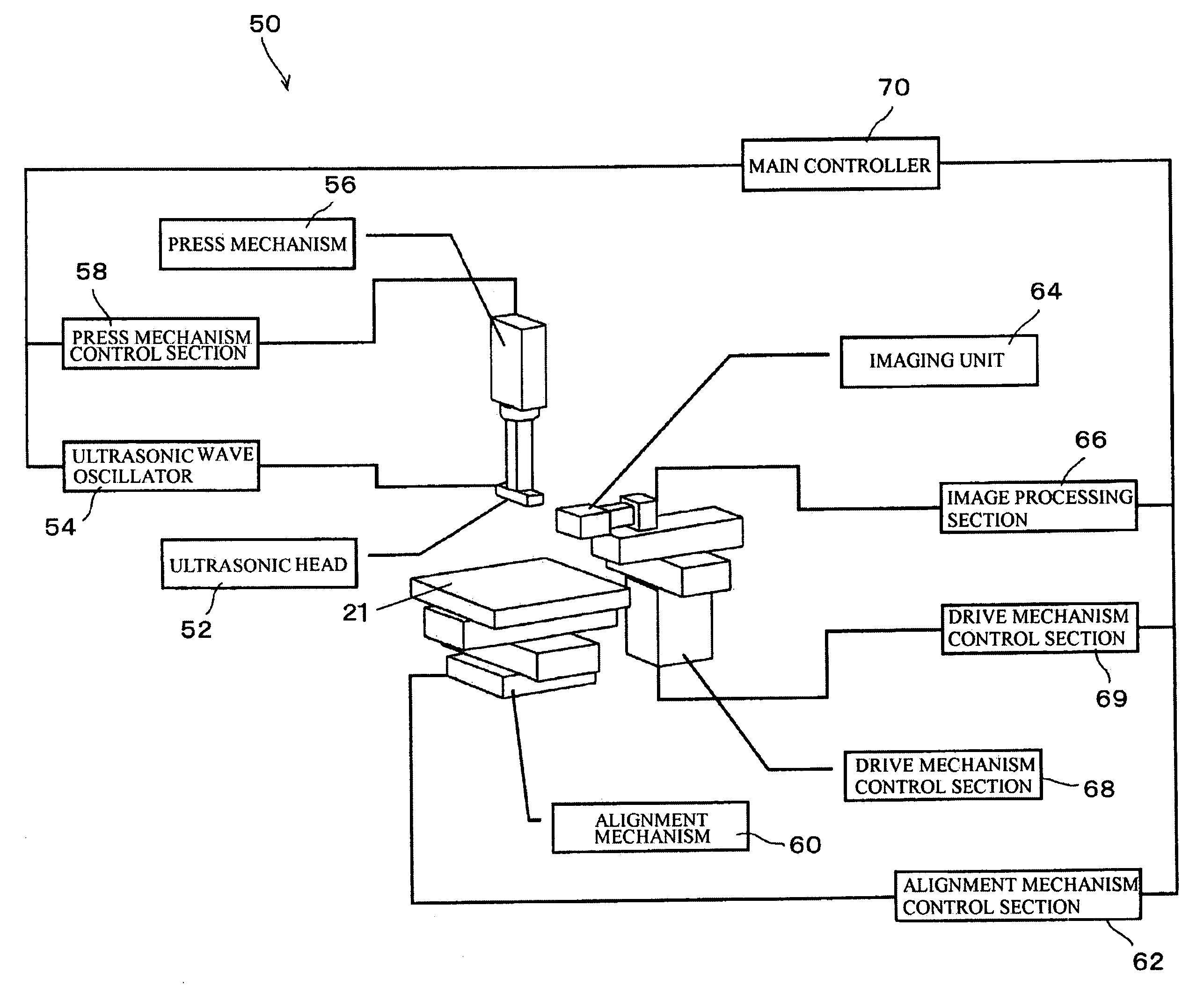
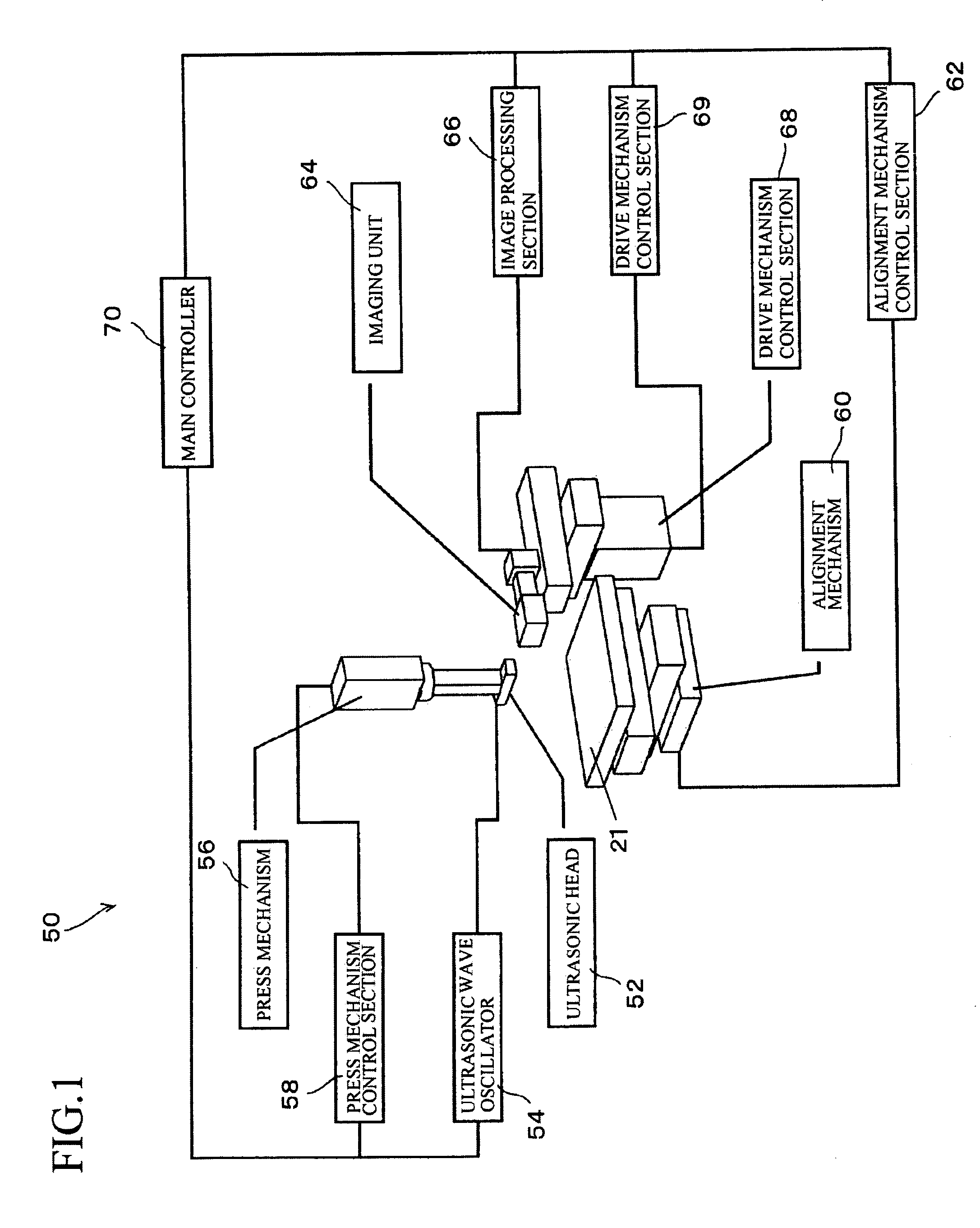
[0040]FIG. 1 shows a mounting machine 50 for flip-chip-bonding a semiconductor chip 10, which is an example of the electronic component, onto a circuit board 20.

[0041]The mounting machine 50 mainly comprises a ultrasonic head side and a supporting table side. The ultrasonic head side includes: a ultrasonic head 52 air-sucking and holding the semiconductor chip 10; a ultrasonic wave oscillator 54 applying ultrasonic vibrations to the ultrasonic head 52; a press mechanism 56 pressing the semiconductor chip 10 toward the circuit board 10; and a press mechanism control section 58 controlling a load of the press mechanism 56.

[0042]On the other hand, the supporting table side includes: an alignment mechanism 60 positioning and moving a supporting table 21 in X- Y- and θ-directions; and an alignment mechanism control section 62 controlling the alignment mechanism...


PUM

PropertyMeasurementUnit
stressaaaaaaaaaa
displacementaaaaaaaaaa
frequencyaaaaaaaaaa

Abstract

The ultrasonic mounting method is capable of uniformly bonding bumps of an electronic component to a circuit board and improving reliability of ultrasonic-mounting the electronic component. The method comprises the step of applying ultrasonic vibrations to the electronic component so as to flip-chip-bond the electronic component to the circuit board having electrodes. The ultrasonic vibrations are applied in a direction parallel to a surface of the electronic component, and loads are vertically applied to the surface of the electronic component in conjunction with vibration cycles of the ultrasonic vibrations.

Description

BACKGROUND OF THE INVENTION[0001]The present invention relates to a method of ultrasonic-mounting an electronic component and a ultrasonic mounting machine.[0002]When a semiconductor chip, which is an example of the electronic component, is mounted on a circuit board by flip chip bonding, bumps of the semiconductor chip are headed for the circuit board, then the bumps, which are made of gold or solder, are respectively bonded to electrodes of the circuit board. A space between the semiconductor chip and the circuit board is filled with synthetic resin so as to protect a circuit face of the semiconductor chip, prevent the bumps from corrosion and improve bonding strength therebetween.[0003]These days, the semiconductor chip is flip-chip-bonded by applying ultrasonic vibrations. By applying ultrasonic vibrations, bonding sections between the bumps and the electrodes are alloyed and bonded.[0004]A method of flip-chip-bonding a semiconductor chip by applying ultrasonic vibrations is sho...

Claims


Application Information

Patent Timeline
Patent Type & Authority Patents(United States)
IPC IPC(8): B32B37/00
CPCB23K20/10B23K20/106H01L21/67144H01L24/75H01L24/81B23K2201/42H01L2224/75H01L2224/75355H01L2224/81205H01L2224/81801H01L2924/01079H01L2924/01005H01L2924/01006H01L2924/01033H01L2924/014B23K2101/42
Inventor MATSUMURA, TAKAYOSHIKIRA, HIDEHIKOKOBAE, KENJIKAINUMA, NORIO
Owner FUJITSU LTD
Why Eureka
Try Eureka