

Semiconductor device and method for evaluating characteristics of the same
An evaluation method, semiconductor technology, applied in the direction of semiconductor devices, semiconductor/solid-state device components, semiconductor/solid-state device testing/measurement, etc., can solve problems that cannot represent the distribution of the main characteristics of semiconductor integrated circuits, and excessively strict management of manufacturing conditions, etc.
- Summary
- Abstract
- Description
- Claims
- Application Information
AI Technical Summary
Problems solved by technology
Method used
Image

Examples
no. 1 Embodiment approach
[0036] —Structure of the Evaluation Department—
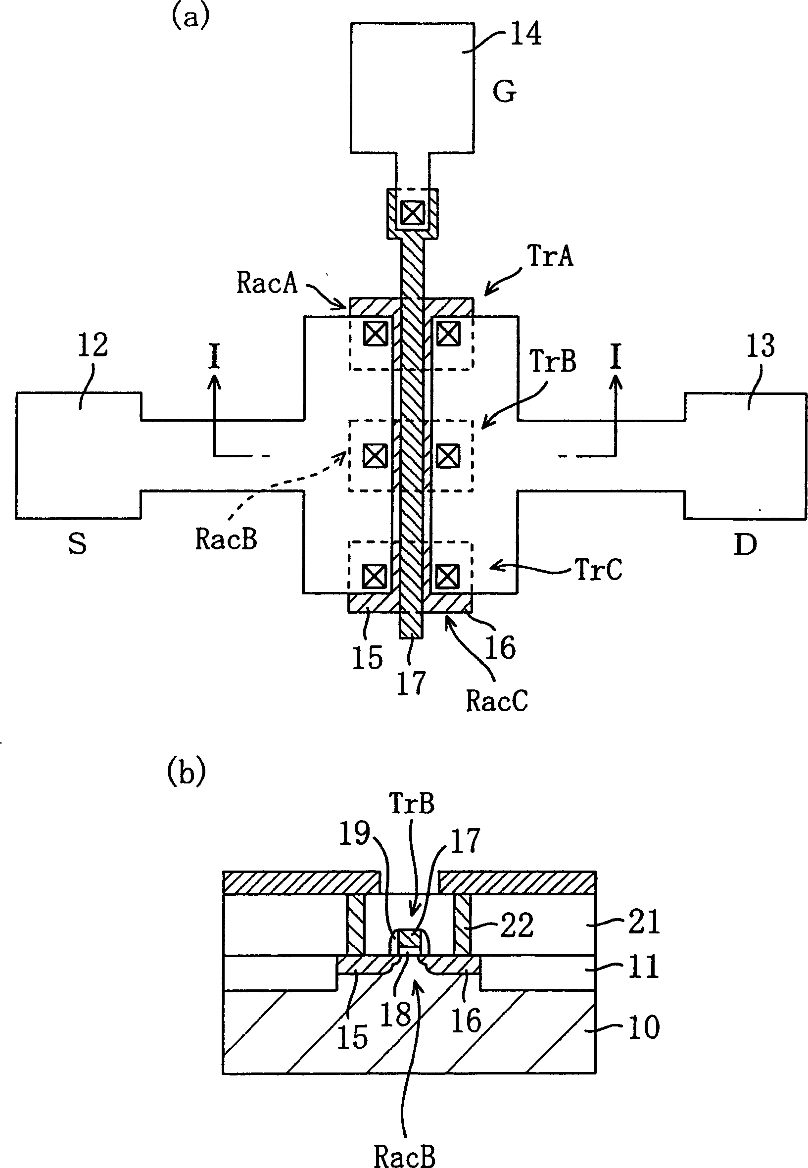
[0037] figure 1 (a) and (b) respectively show a plan view of an evaluation unit in the semiconductor device according to the first embodiment, and an I-I line cross-sectional view of one MIS transistor for evaluation in the evaluation unit, respectively.
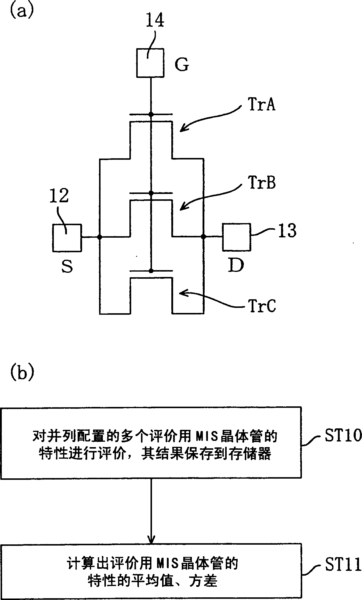
[0038] Such as figure 1 As shown in (a) and (b), the evaluation section is configured by arranging MIS transistors TrA, TrB, and TrC for evaluation, which are elements for characteristic evaluation, on the three active regions RacA, RacB, and RacC surrounded by the trench element isolation 11. . Furthermore, the common gate electrode 17 is provided on the three evaluation MIS transistors TrA to TrC. In addition, the evaluation section further includes a source pad 12 (common conductor portion for source) electrically connected to the respective source regions 15 of the three MIS transistors TrA-TrC for evaluation, and a source pad 12 (common conductor portion for source)...
no. 2 Embodiment approach
[0053] Figure 4 (a) and (b) are respectively a plan view of the evaluation unit of the semiconductor device according to the second embodiment and a cross-sectional view of one MIS transistor for evaluation in the evaluation unit taken along line IV-IV, respectively.
[0054] Such as Figure 4 As shown in (a) and (b), in the present embodiment, the evaluation unit arranges the evaluation MIS transistors TrA, TrA, and TrB, TrC constituted. Furthermore, the common gate electrode 17 is provided on the three evaluation MIS transistors TrA to TrC. In addition, the evaluation section further includes source pads 12 electrically connected to the source regions 15 of the three MIS transistors TrA to TrC for evaluation, and pads 12 electrically connected to the drain regions 16 of the three MIS transistors TrA to TrC for evaluation. The drain pad 13 and the gate pad 14 are electrically connected to the common gate electrode 17 on the three evaluation MIS transistors TrA to TrC.
...
no. 3 Embodiment approach
[0063] Figure 5 (a) and (b) are, respectively, a plan view of an evaluation unit in the semiconductor device according to the third embodiment, and a cross-sectional view of one of the evaluation MIS transistors in the evaluation unit taken along line V-V.
[0064] Such as Figure 5 As shown in (a) and (b), in this embodiment, the evaluation unit is configured by arranging the evaluation MIS transistor TrA, which is the element for characteristic evaluation, on the three active regions RacA, RacB, and RacC surrounded by the trench element isolation 11. , TrB, TrC. Furthermore, the common gate electrode 17 is provided on the three evaluation MIS transistors TrA to TrC. In addition, the evaluation section further includes source pads 12 electrically connected to the source regions 15 of the three MIS transistors TrA to TrC for evaluation, and pads 12 electrically connected to the drain regions 16 of the three MIS transistors TrA to TrC for evaluation. The drain pad 13 and th...
PUM
 Abstract
Description
Claims
Application Information