

Amplification circuit
A technology for amplifying circuits and voltage sources, applied in amplifiers, logic circuits, single-ended push-pull amplifiers, etc., can solve problems such as insufficient dynamic range, reduce circuit scale, simplify circuit structure, and realize integration Effect
- Summary
- Abstract
- Description
- Claims
- Application Information
AI Technical Summary
Problems solved by technology
Method used
Image

Examples
Embodiment approach 1
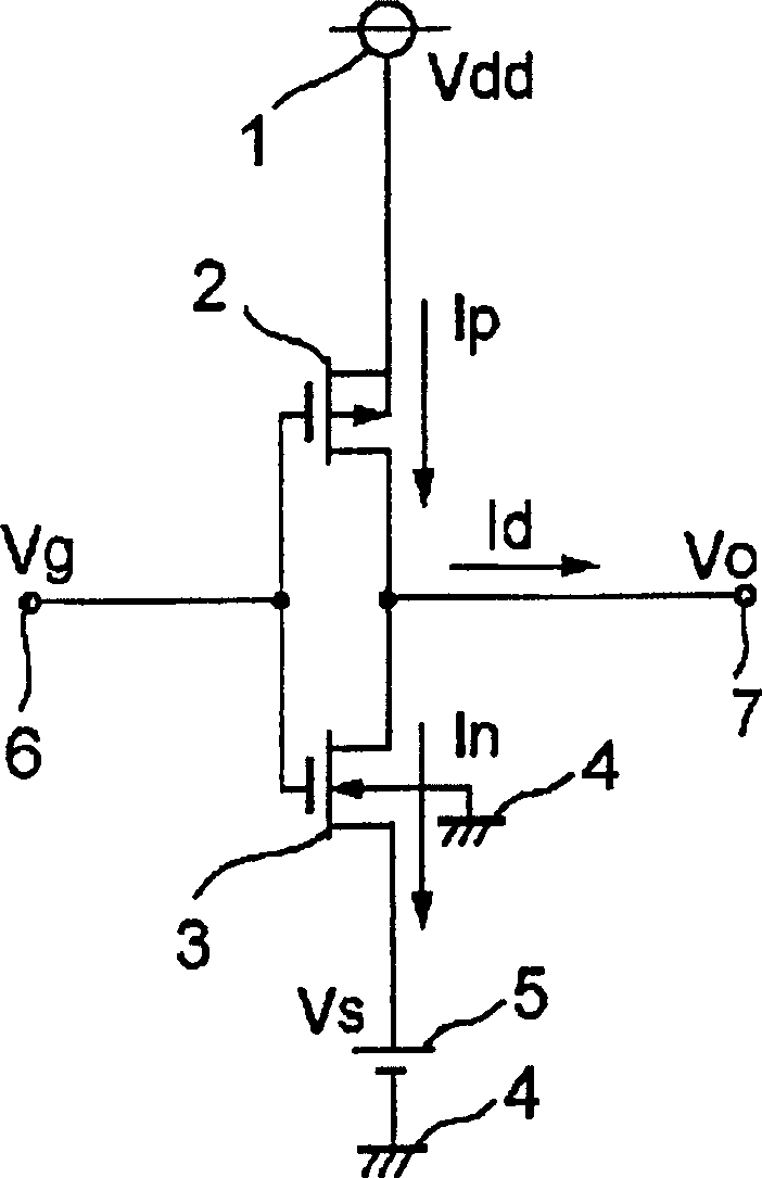
[0051] figure 1 It is a diagram showing the operating principle of the DC offset detection circuit of the present invention. exist figure 1 Among them, 1 is a voltage source, 2 is a PMOS transistor (the third PMOS transistor), 3 is an NMOS transistor (the third NMOS transistor), 4 is a ground terminal, and 5 is inserted between the source of the NMOS transistor 3 and the ground terminal 4 to make the NMOS The source voltage of transistor 3 is raised to reduce the voltage source for DC offset, 6 is the input terminal and 7 is the output terminal. In addition, the back gate of the PMOS transistor 2 is connected to the source, and the back gate of the NMOS transistor 3 is connected to the ground terminal 4 . Furthermore, assuming that the voltage value of the voltage source 1 is Vdd, the drain current of the PMOS transistor is Ip, the drain current of the NMOS transistor is In, the current flowing to the output terminal 7 is Id, and the voltage value of the voltage source 5 (...
Embodiment approach 2
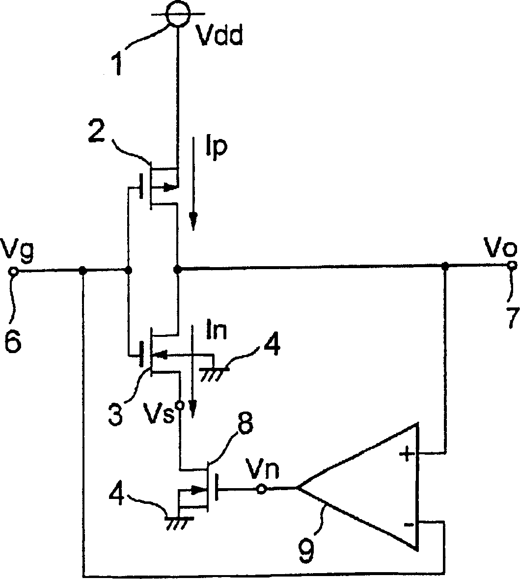
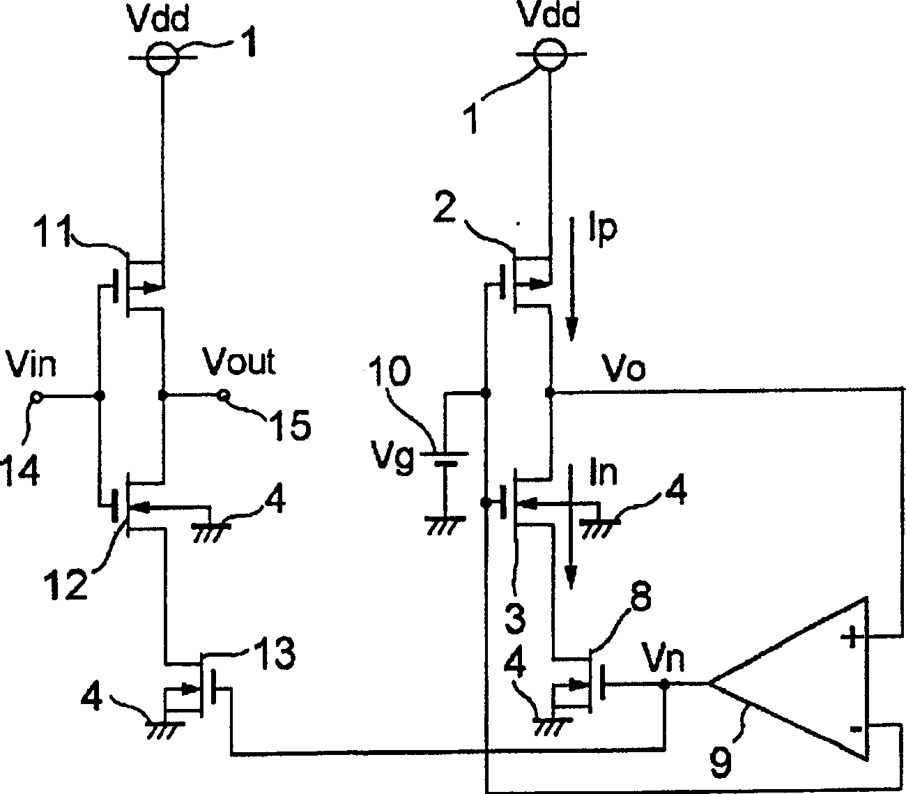
[0103] 6 is a circuit diagram showing the configuration of an amplifier circuit according to Embodiment 2 of the present invention. As mentioned above, when operating from a single power supply, image 3 The amplifying circuit shown can remove the DC offset when Vtp≥Vtn and Mp≤Mn. On the other hand, FIG. 6 shows that the amplifier circuit according to the second embodiment of the present invention can remove the DC offset when VtpMn, which is different from the amplifier circuit according to the first embodiment. In Figure 6, due to and image 3 The same symbols denote the same or corresponding parts, so descriptions thereof are omitted. 61 is a PMOS transistor (second PMOS transistor) inserted between the source of the PMOS transistor 11 and the voltage source 1 in order to reduce the source voltage of the PMOS transistor 11 to remove the DC offset, and 62 is formed and inserted in the same manner as the PMOS transistor 61. In the PMOS transistor (the 4th PMOS transistor) ...
Embodiment approach 3
[0116] The amplifier circuit according to Embodiment 3 of the present invention is for image 3 The first voltage bias means raises the source voltage of the NMOS transistor constituting the CMOS inverter circuit as shown, and the second voltage bias means reduces the source voltage of the PMOS transistor constituting the CMOS inverter circuit as shown in FIG. The shifting device is different from Embodiment 1 and Embodiment 2 in that two voltage shifting devices are combined with a simple configuration by providing a common part. Figure 9 It is a circuit diagram showing the configuration of an amplifier circuit according to Embodiment 3 of the present invention. exist Figure 9 in, due to image 3 The same reference numerals as in FIG. 6 denote the same or corresponding parts, and description thereof will be omitted.
[0117] Second, specify Figure 9 Operation of the amplifier circuit shown. In the case of Vtp≥Vtn and Mp≤Mn, the operational amplifier 9 functions, and t...
PUM
 Abstract
Description
Claims
Application Information