
Liquid crystal panel, liquid crystal display device, and electronic equipment

A liquid crystal display, liquid crystal panel technology, applied in liquid crystal materials, static indicators, instruments, etc., can solve the problems of uneven surface of indium tin electrodes, difficult to respond to actual output speed, etc.

Inactive Publication Date: 2005-02-02
NEC LCD TECH CORP
View PDF1 Cites 3 Cited by
  • Summary
  • Abstract
  • Description
  • Claims
  • Application Information

AI Technical Summary

Problems solved by technology

In this case, even if the surface of the indium tin electrode, which is the transparent electrode, is slightly uneven, it is problematic
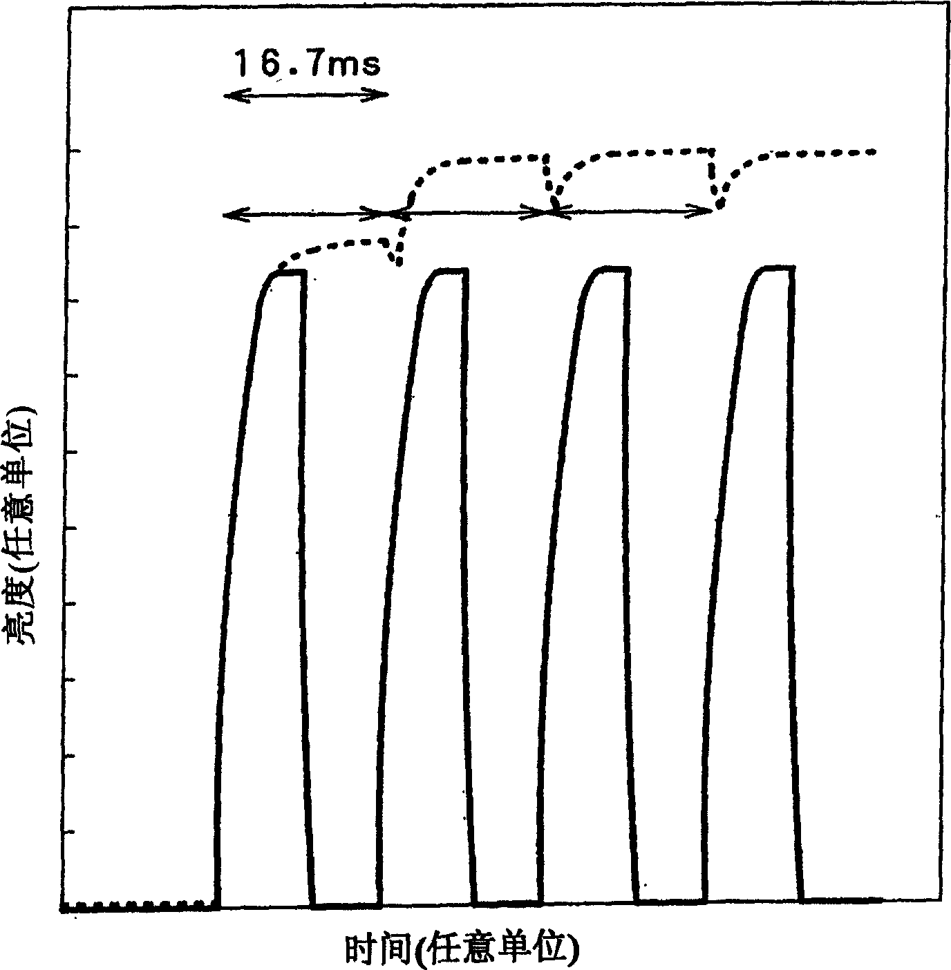
[0061] According to this method, it is difficult for all the traditional methods mentioned above to further improve the response speed while maintaining the actual output.

Method used


Image

  • Liquid crystal panel, liquid crystal display device, and electronic equipment
  • Liquid crystal panel, liquid crystal display device, and electronic equipment
  • Liquid crystal panel, liquid crystal display device, and electronic equipment

Examples


Embodiment Construction

[0096] Embodiments of the present invention will be described in detail with reference to the drawings. Now, a first embodiment of the present invention will be described. Image 6 A cross-sectional view of a unit structure of a TFT array in a liquid crystal panel according to an embodiment of the present invention is given. Image 6 The TFT array shown is a polysilicon TFT array formed by converting amorphous silicon to polysilicon.

[0097] Such as Image 6 As shown, the polysilicon TFT has a structure in which a silicon oxide film 28 is formed on a glass substrate 29 and a polysilicon layer is partially formed thereon. The polysilicon layer is formed by depositing amorphous silicon on the silicon oxide layer 28, thereafter converting the amorphous silicon to polysilicon by annealing with an excimer laser, and thereafter patterning the polysilicon. A gate oxide film was formed at a thickness of 10 nm on the surface of the polysilicon layer. exist Image 6 Among them, the ga...


PUM

PropertyMeasurementUnit
transmittivityaaaaaaaaaa

Abstract

A relation between a twist pitch p of twisted nematic liquid crystal and a thickness d of a liquid crystal layer is set to p / d<8, and polymer stabilization is carried out. In this way, torque to recover from alignment upon application of a voltage to alignment without application of the voltage is increased and response speed of the liquid crystal at decay time is thereby increased. By applying the present technique to a liquid crystal display device which is driven by a reset operation, an overdrive operation or common modulation, high response speed is obtained even when the twisted nematic liquid crystal is used. As a result, the liquid crystal display device can deal with field sequential display mode where higher response speed is required.

Description

technical field [0001] The invention relates to a liquid crystal panel, a liquid crystal display using the liquid crystal panel, and electronic equipment using the liquid crystal display. Background technique [0002] With the development of the multimedia era, which ranges from small devices used in projectors, cellular phones, etc. to large devices used in laptop personal computers, monitors, televisions, etc., the rapid spread of liquid crystal displays . Meanwhile, medium-sized liquid crystal displays are indispensable for electronic devices such as televisions or personal digital assistants (PDAs), and entertainment devices such as portable game machines and pachinko machines (pinball machines in Japan). In addition, liquid crystal displays can be used in many other devices including household appliances such as refrigerators, microwave ovens, and the like. [0003] Currently, most liquid crystal display elements adopt a twisted nematic (TN) display mode. A liquid cr...

Claims


Application Information

Patent Timeline
Patent Type & Authority Applications(China)
IPC IPC(8): C09K19/02G02F1/133G02F1/1337G02F1/1345G02F1/1368G02F1/137G02F1/139G09G3/20G09G3/36
CPCC09K19/0208G02F1/1396G02F2001/13775G02F1/13775
Inventor 高取宪一斯维特拉娜·A·克什克哈娜
Owner NEC LCD TECH CORP
Learn More