Electrical contacting method

A technology of conductive connection and wire line, applied in the direction of the formation of electrical connection of printed components, printed circuits, electrical components, etc., can solve the problems of large space, unsuitable, expensive, etc., and achieve the effects of cost saving, space saving, and mechanical stability

Inactive Publication Date: 2005-02-02
NOVAR PLC
View PDF0 Cites 2 Cited by
  • Summary
  • Abstract
  • Description
  • Claims
  • Application Information

AI Technical Summary

Problems solved by technology

[0003] However, MID-components are not suitable as a substitute for a general-purpose printed circuit board or circuit board on which a large number of electronic components with a high packing density and a very small conductor line pitch are arranged in the SMD process, which often occurs in this case The problem that one or more circuit boards are conductively connected with a MID-member
Previous methods, namely soldering in jumper wires or mechanically conductive connections via plug-in terminals, spring terminals, conductive rubber strips, etc., are material-intensive and, on the other hand, take up a lot of space, are expensive and take up valuable manufacturing time

Method used


Image

  • Electrical contacting method
  • Electrical contacting method
  • Electrical contacting method

Examples


Embodiment Construction

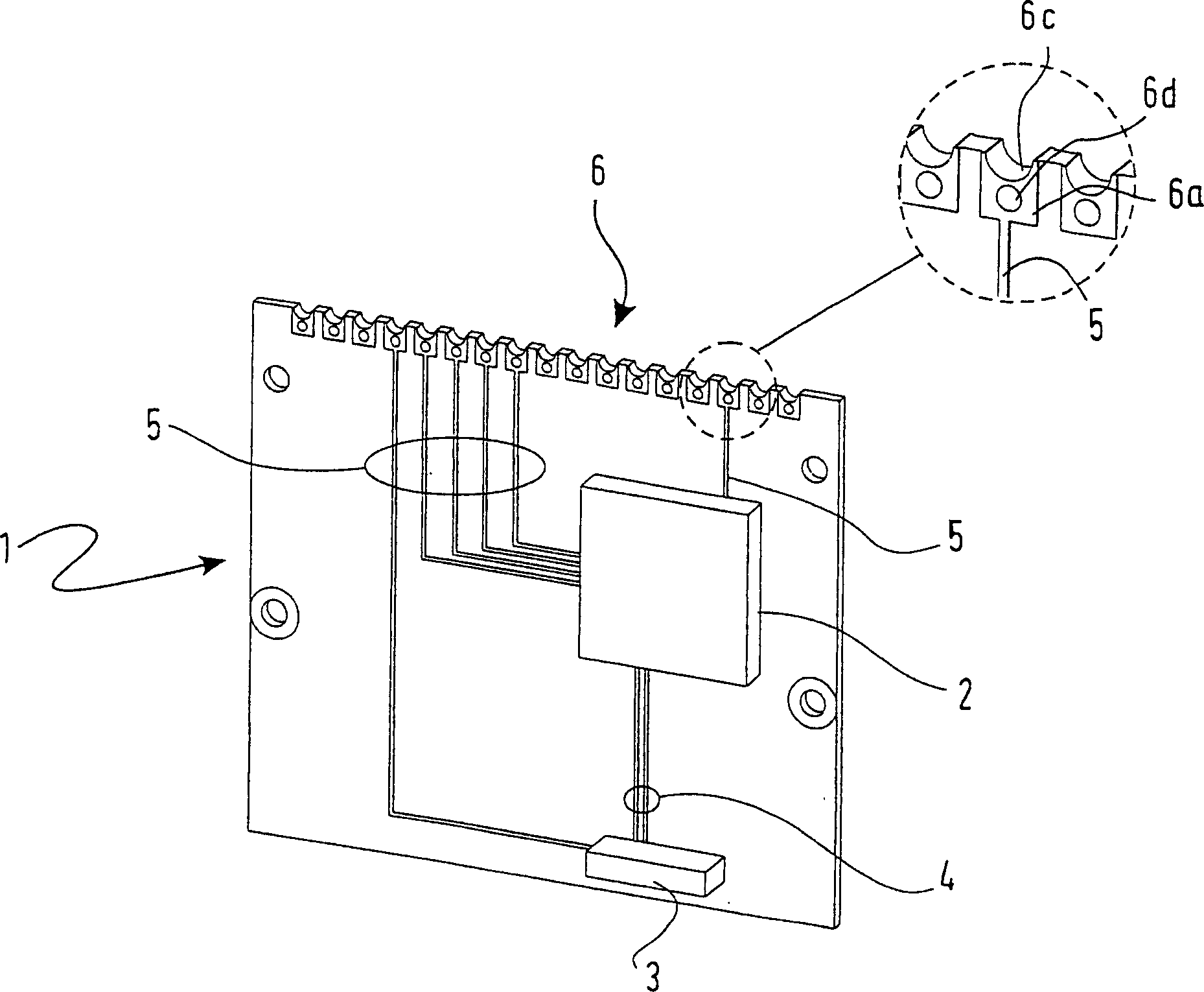
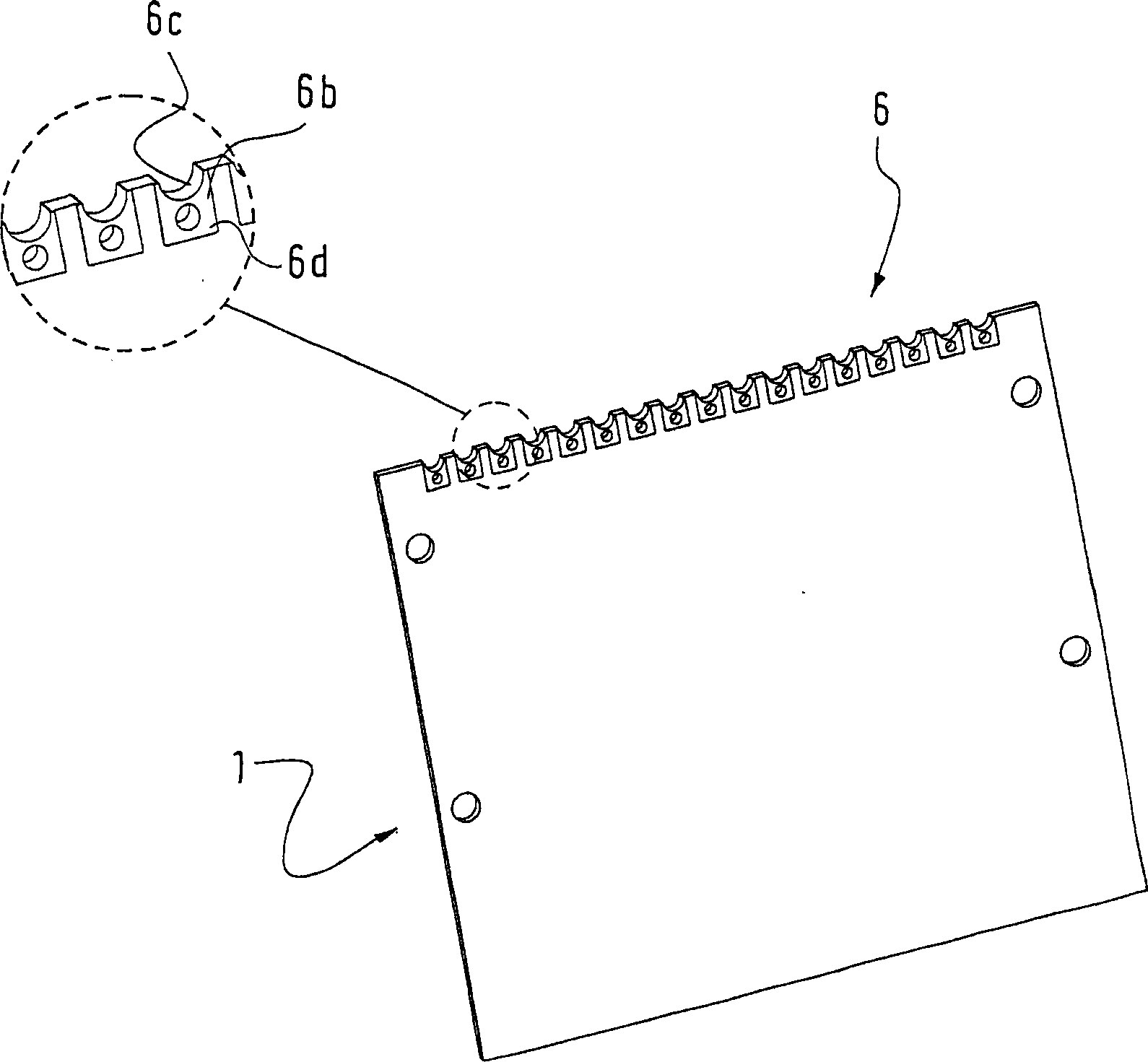
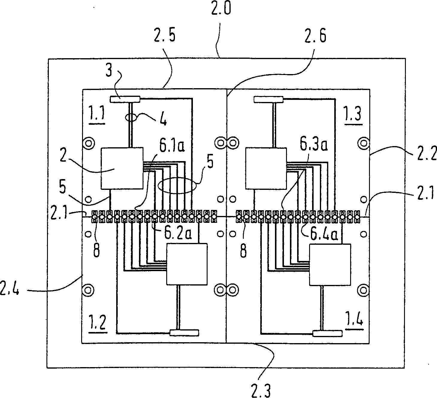
[0029] figure 1 In a simplified perspective view, a printed circuit board, for example made of glass-fiber-reinforced epoxy resin, is shown, which is provided with components 2 and 3 , which are here only indicated by symbols, and which are connected to one another by conductor tracks 4 . The power and signal line connections of the components 2 and 3 lead via a further conductor path 5 to an edge contact 6 at the upper edge of the printed circuit board. There, the individual conductor tracks diverge into the widened conductive connection area 6a, see enlarged detail. The conductive connection areas 6a are arranged in a defined grid along almost the entire upper edge of the printed circuit board 1 and do not require outgoing conductive connections. The back side of the circuit board 1 can also be provided with wire lines and equipped with electrical components.

[0030] Even if, as in this embodiment, the wiring board is only provided with wiring lines and components on the ...


PUM


Abstract

A method for contacting printed conductors terminating at the edge of a circuit board with printed conductors of a MID component includes: on a panel which includes the circuit board, producing the printed conductors of the circuit board in a layout in which the printed conductors are extended past a partition line which defines the edge of the circuit board; providing the panel with through holes along the partition line in the region of the printed conductors; electroplating through the through holes; and positioning the circuit board in relation to the MID component and soldering the printed conductors of the circuit board to the printed conductors of the MID component. Rear electrical contacting areas are provided on a back side of the panel near the partition line, and the printed conductors are connected to the rear electrical contacting areas via the through holes.

Description

technical field [0001] The invention relates to a method for electrically conductively connecting at least one conductor track terminated at the edge of a printed circuit board with a conductor track located on an adjacent component made of thermoplastic material using the MID process. Background technique [0002] As so-called Molding Injection Devices (MID), ie electrical components produced using the MID process can be structured directly by laser according to different methods, e.g. masking, by two-component injection molding with subsequent galvanic metallization , post-spraying (Hinterspritzen) film or hot embossing with the desired conductor lines. The MID components produced in this way—unlike ordinary circuit boards made of GFK etc.—are three-dimensional shaped parts with built-in wiring layouts and in some cases other electronic or electromechanical components. Using this type of MID-component, even if it is only provided with conductor lines and used as a substit...

Claims


Application Information

Patent Timeline
Patent Type & Authority Applications(China)
IPC IPC(8): H05K1/00H05K3/00H05K3/34H05K3/36H05K3/40H05K3/42
CPCH05K3/403H05K2201/09481H05K3/42H05K2201/09118H05K3/368H05K2203/0455H05K2201/10666H05K3/3405H05K2201/09181H05K3/0052H05K3/3442H05K1/0284Y10T29/49144Y10T29/49165Y10T29/49117Y10T29/49126Y10T29/49789Y02P70/50
Inventor A·格恩哈特T·古勒特C·门策尔W·奥利科
Owner NOVAR PLC
Why Eureka
Try Eureka