LED structure

A technology of light-emitting diodes and light-emitting chips, which is applied to semiconductor devices of light-emitting elements, light sources, cooling/heating devices of lighting devices, etc., and can solve problems such as poor heat dissipation, fewer light-emitting chips, and inability to apply general lighting

Inactive Publication Date: 2005-03-30
FUJIAN JOINLUCK ELECTRONICS ENTERPRISE
View PDF0 Cites 20 Cited by
  • Summary
  • Abstract
  • Description
  • Claims
  • Application Information

AI Technical Summary

Problems solved by technology

[0002] The traditional packaging technology of light-emitting diode (LED) is to fix the light-emitting chip on the bracket with crystal-bonding glue, then connect the metal wire between the light-emitting chip and the bracket, and then encapsulate it with epoxy resin. The plug-in method is soldered and fixed on the printed circuit board. This structure of the light-emitting diode is dissipated by the bracket, and the heat dissipation effect is poor. The junction temperature of the light-emitting chip is high, which will affect the luminous efficiency and life of the light-emitting diode.
Moreover, this light-emitting diode structure has fewer light-emitting chips distributed per unit area, so it cannot be applied to general lighting that requires higher brightness.

Method used


Image

  • LED structure
  • LED structure
  • LED structure

Examples


Embodiment Construction

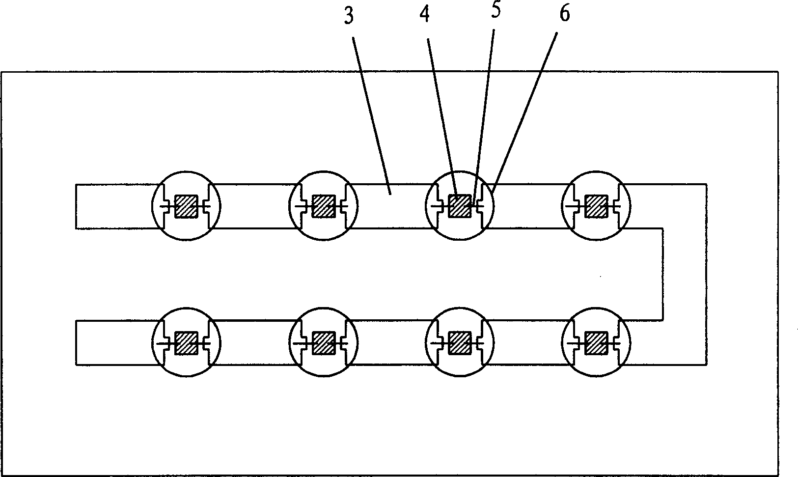
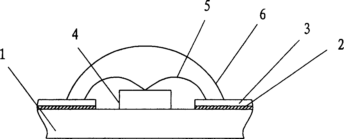
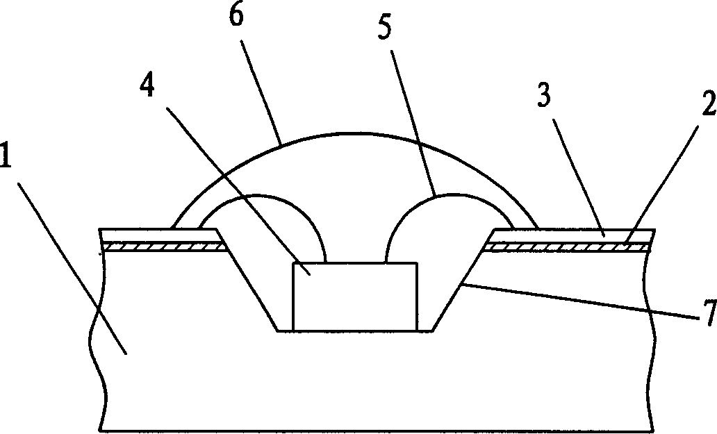
[0025] refer to figure 1 , figure 2 As shown, the light-emitting diode structure includes a heat-conducting substrate 1, and a circuit 3 is arranged on the heat-conducting substrate 1. There is an insulating layer 2 between the heat-conducting substrate 1 and the circuit 3, and more than one light-emitting chip 4 is distributed between the circuits 3. In the space on the substrate 1 , the light-emitting chip 4 is connected to the circuit 3 through the metal wire 5 , and the light-emitting chip 4 is covered with a light-transmitting protective layer 6 .

[0026] The thermally conductive substrate 1 is made of aluminum, copper, and ceramics with good thermal conductivity. Of course, other materials with good thermal conductivity can also be used; the insulating layer 2 should have strong insulating properties, and the circuit 3 covered on the insulating layer 2 can be copper. Foil, by first covering the insulating layer 2 with a layer of copper foil, and then making various re...


PUM


Abstract

Structure of the disclosed LED raises effect of heat elimination remarkably, reduces junction temp of luminescence chip, and raises luminous efficacy and lifetime of LED. Also the disclosed LED increases quantity of luminescence chip in unit area and luminous efficiency in unit area. Structure of LED is as following: circuits are setup at heat conducting base plate; there is a insulating layer between heat conducting base plate and circuit, and more than one luminescence chips are distributed among circuits; chips through metal wires are connected to circuit, and photic protection layer is covered on the luminescence chips. The heat conducting base plate reduces junction temp, raises efficiency and life time of chip as well as makes more chips possible be arranged on unit area.

Description

technical field [0001] The present invention relates to light emitting diode structures. Background technique [0002] The traditional packaging technology of light-emitting diode (LED) is to fix the light-emitting chip on the bracket with crystal-bonding glue, then connect the metal wire between the light-emitting chip and the bracket, and then encapsulate it with epoxy resin. The plug-in method is welded and fixed on the printed circuit board. The light-emitting diode of this structure is dissipated by the bracket, and the heat dissipation effect is poor. The junction temperature of the light-emitting chip is high, which will affect the luminous efficiency and life of the light-emitting diode. Moreover, this light-emitting diode structure has fewer light-emitting chips distributed per unit area, so it cannot be applied to general lighting that requires higher brightness. Therefore, reducing the junction temperature of the light-emitting chip to improve the luminous effici...

Claims


Application Information

Patent Timeline
Patent Type & Authority Applications(China)
IPC IPC(8): F21K99/00H01L23/28H01L25/075H01L27/15H01L33/00
CPCH01L25/0753F21K9/00H01L2224/48091H01L2924/12041F21V29/677F21V29/76H01L2924/00014
Inventor 黄德森
Owner FUJIAN JOINLUCK ELECTRONICS ENTERPRISE
Why Eureka
Try Eureka