Quantum well semiconductor and manufacturing method thereof

A manufacturing method and semiconductor technology, applied in semiconductor devices, electrical components, circuits, etc., can solve the problems of low luminous efficiency of medium and large-sized chips, reduce junction temperature, prevent excessive reverse current, and reduce forward voltage Effect

Active Publication Date: 2013-07-31
XIANGNENG HUALEI OPTOELECTRONICS
View PDF4 Cites 13 Cited by
  • Summary
  • Abstract
  • Description
  • Claims
  • Application Information

AI Technical Summary

Problems solved by technology

[0004] The present invention aims to provide a quantum well semiconductor and its manufacturing method to solve the problem of low luminous efficiency of medium and large-sized chips prepared from semiconductor epitaxial wafers with sapphire as the substrate in the prior art

Method used


Image

  • Quantum well semiconductor and manufacturing method thereof
  • Quantum well semiconductor and manufacturing method thereof
  • Quantum well semiconductor and manufacturing method thereof

Examples


Embodiment 1

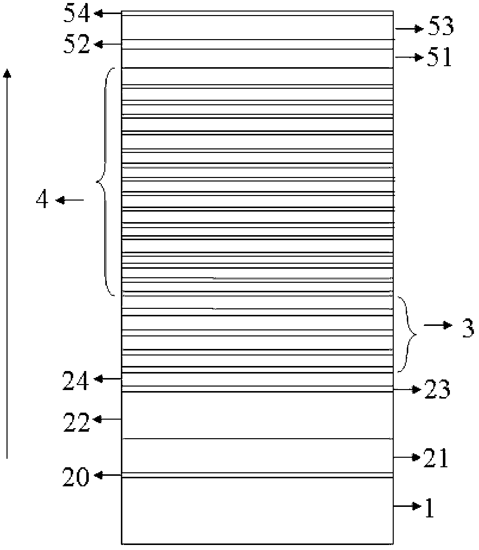
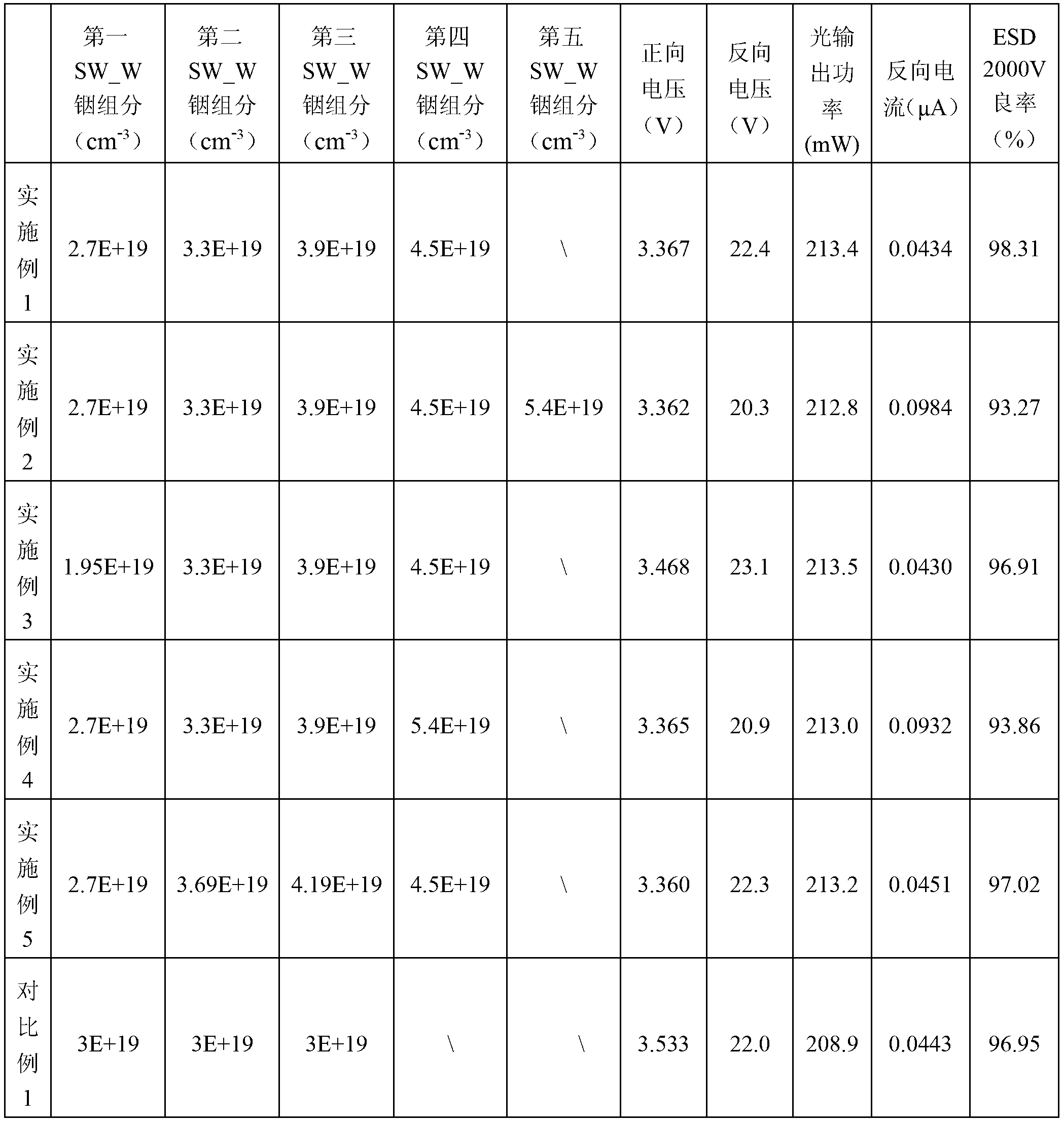
[0039] Prepare the C-plane sapphire patterned substrate, place it on the graphite disk of the AIXTRON Crius1 type MOCVD reaction chamber, and perform heat treatment for 8 minutes at the substrate setting temperature of 1280°C in a hydrogen environment, and then lower the substrate setting temperature to Up to 640°C, the growth pressure is controlled at 450 Torr, trimethylgallium with a flow rate of 60 sccm and high-purity ammonia gas with a flow rate of 10,000 sccm are introduced for 2.5 minutes to form a GaN buffer layer with a thickness of about 45 nm; set the temperature to 1230°C , the growth pressure is controlled at 225 Torr, and the trimethylgallium with a flow rate of 200 sccm and the high-purity ammonia gas with a flow rate of 24000 sccm are fed again to form an undoped GaN layer with a thickness of 3000 nm; the growth pressure is controlled at 113 Torr, and the set temperature is raised to 1240°C, add 16 sccm monomethylsilane gas to the above-mentioned trimethylgalliu...

Embodiment 2

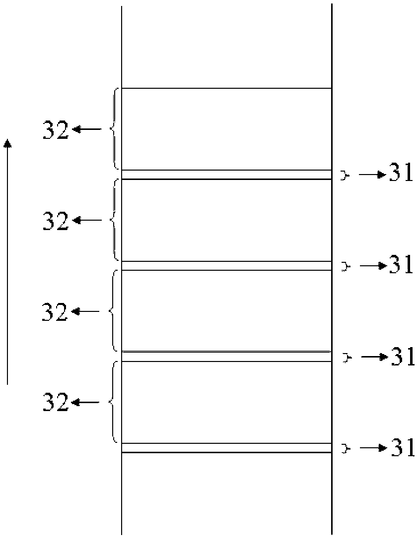
[0043] Form the GaN buffer layer, the undoped GaN layer, the doped GaN layer, the N-type AlGaN electron blocking layer, and the GaN barrier layer protection layer sequentially on the C-face sapphire patterned substrate according to the same method as in Example 1; When the set temperature is maintained at 920°C and the growth pressure is controlled at 225Torr, the first InGaN with a thickness of 0.8nm is formed by passing high-purity ammonia gas with a flow rate of 33000sccm, triethylgallium with a flow rate of 40sccm, and trimethylindium with a flow rate of 351sccm. layer, and then fed trimethylgallium with a flow rate of 95 sccm and monomethylsilane gas with a flow rate of 0.68 sccm to form the first GaN layer with a thickness of 40 nm, and trimethyl indium with a flow rate of 429 sccm to form the first GaN layer with a thickness of 0.8 nm. Two InGaN layers, repeating the process of forming the first GaN layer to form a second GaN layer with a thickness of 40nm, feeding trime...

Embodiment 3

[0045] Form the GaN buffer layer, the undoped GaN layer, the doped GaN layer, the N-type AlGaN electron blocking layer, and the GaN barrier layer protection layer sequentially on the C-face sapphire patterned substrate according to the same method as in Example 1; When the set temperature is maintained at 920°C and the growth pressure is controlled at 225Torr, the first InGaN with a thickness of 0.8nm is formed by passing high-purity ammonia gas with a flow rate of 33000 sccm, triethylgallium with a flow rate of 40 sccm and trimethyl indium with a flow rate of 254 sccm layer, and then fed trimethylgallium with a flow rate of 95 sccm and monomethylsilane gas with a flow rate of 0.68 sccm to form the first GaN layer with a thickness of 40 nm, and trimethyl indium with a flow rate of 429 sccm to form the first GaN layer with a thickness of 0.8 nm. Two InGaN layers, repeating the process of forming the first GaN layer to form a second GaN layer with a thickness of 40nm, feeding tri...


PUM


Abstract

The invention provides a quantum well semiconductor and a manufacturing method thereof. The quantum well semiconductor comprises a substrate, a shallow quantum well layer and a multiple quantum well light emitting layer that are arranged in sequence from inside to outside, wherein the shallow quantum well layer comprises at least four InGaN layers and GaN layers; the InGaN layer close to the substrate is a first InGaN layer; the number of the GaN layers is the same as that of the InGaN layers; the GaN layers and the InGaN layers are superposed in a crossed manner; the GaN layer close to the substrate is a first GaN layer; the first GaN layer is arranged between the substrate and the first InGaN layer; the content of In in the first InGaN layer is 1.95E+19-2.7E+19cm<-3>; and the content of In in each of all the InGaN layers except the first InGaN layer is greater than 3.0E+19cm<-3> and is increased gradually in the direction far away from the substrate. The shallow quantum well layer can prevent excessive reverse current, facilitates pass-through of electrons, reduces the forward voltage and heat productivity of a chip during operation, and improves the light emitting efficiency.

Description

technical field [0001] The invention relates to the field of semiconductors, in particular to a quantum well semiconductor and a manufacturing method thereof. Background technique [0002] With sapphire (Al 2 o 3 ) as the substrate semiconductor epitaxial wafer is mainly suitable for the preparation of small and medium-sized chips, and the main application fields are small-sized liquid crystal backlight, digital display, toys, instruments, etc. Due to the problems of low luminous efficiency due to current congestion and difficulty in heat dissipation, it is difficult to use it as a lighting chip. At present, the medium and large size chips required for lighting mainly rely on imported semiconductor epitaxy with SiC as the substrate. The cost of the lighting device is greatly increased. [0003] Therefore, considering the low cost of the semiconductor epitaxial wafer with sapphire as the substrate, if the heat dissipation effect and light output power can be improved, the ...

Claims


Application Information

Patent Timeline
Patent Type & Authority Applications(China)
IPC IPC(8): H01L33/06H01L33/14H01L33/32H01L33/00
Inventor 伍毅龙谭桂英王新建
Owner XIANGNENG HUALEI OPTOELECTRONICS
Why Eureka
Try Eureka