Low-voltage punch-through bi-directional transient-voltage suppression devices having surface breakdown protection and methods of making the same

A transient voltage suppression and device technology, which is applied in semiconductor/solid-state device manufacturing, electrical solid-state devices, semiconductor/solid-state device components, etc., can solve problems such as increasing costs, and achieve the effect of preventing surface breakdown

Inactive Publication Date: 2005-04-06
GEN SEMICON
View PDF2 Cites 12 Cited by
  • Summary
  • Abstract
  • Description
  • Claims
  • Application Information

AI Technical Summary

Problems solved by technology

Obviously, this layout adds cost by requiring more than one device to achieve the intended function

Method used


Image

  • Low-voltage punch-through bi-directional transient-voltage suppression devices having surface breakdown protection and methods of making the same
  • Low-voltage punch-through bi-directional transient-voltage suppression devices having surface breakdown protection and methods of making the same
  • Low-voltage punch-through bi-directional transient-voltage suppression devices having surface breakdown protection and methods of making the same

Examples


Embodiment Construction

[0027] Those skilled in the art will be able to realize that the following description is illustrative only and not limiting. Other embodiments of the invention will be readily apparent to the skilled artisan.

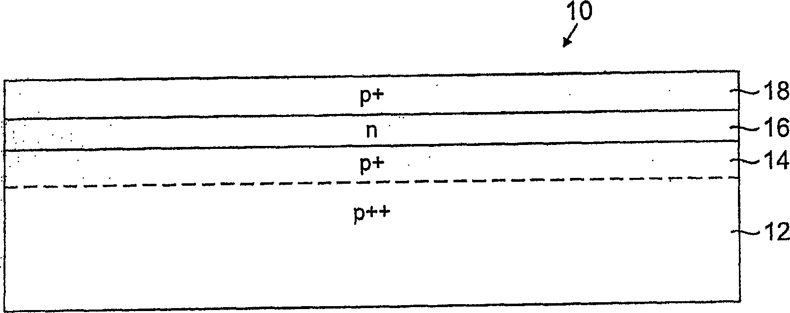
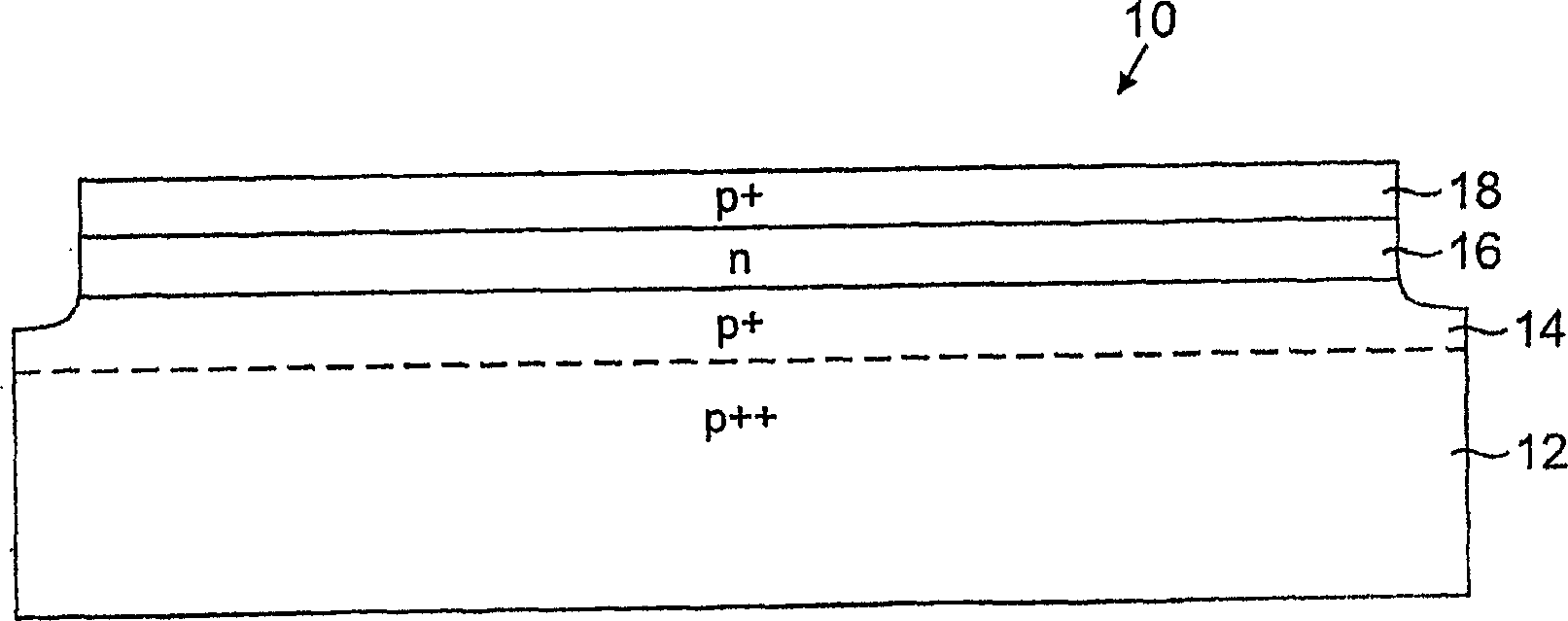
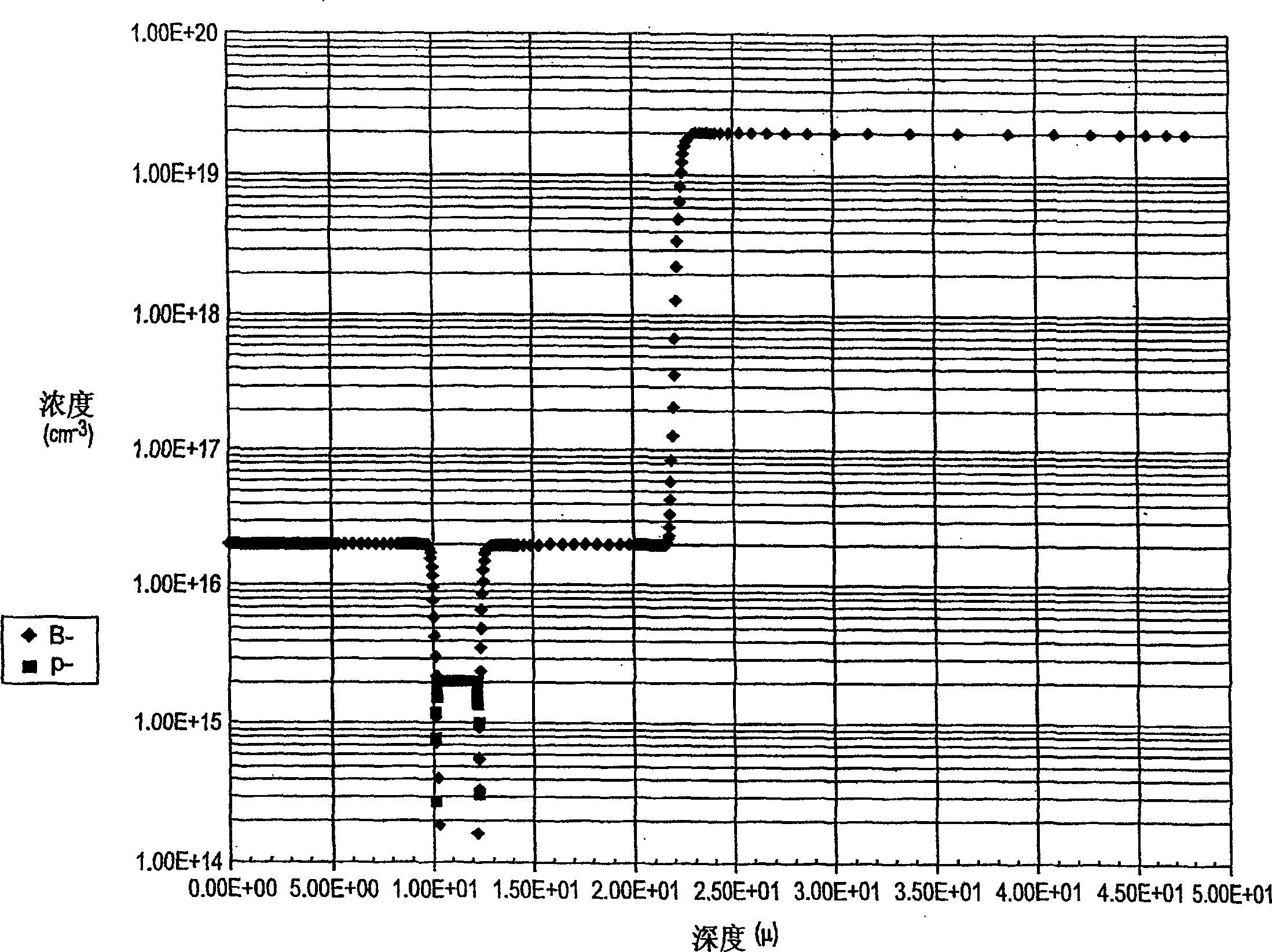
[0028] refer to figure 1, schematically shows a p++p+np+ three-layer epitaxial punch-through bidirectional transient voltage suppressor 10 according to the present invention with a cross-sectional view. The device of the present invention is formed on a p++ semiconductor substrate 12 . On the p++ substrate, three regions are grown epitaxially, preferably in one continuous process. First epitaxial p+ region 14 is initially formed on the upper surface of p++ region 12 . Epitaxial n region 16 is then formed on the upper surface of p+ region 14 and a second epitaxial p+ region 18 is formed on the upper surface of n region 16 . A p++ ohmic contact (not shown) is typically provided on the upper surface of p+ region 18 . This device contains two junctions: (1) the juncti...


PUM


Abstract

A method of making a bi-directional transient voltage suppression device is provided, which comprises: (a) providing a p-type semiconductor substrate; (b) epitaxially depositing a lower semiconductor layer of p-type conductivity; (c) epitaxially depositing a middle semiconductor layer of n-type conductivity over the lower layer; (d) epitaxially depositing an upper semiconductor layer of p-type conductivity over the middle layer; (e) heating the substrate, the lower epitaxial layer, the middle epitaxial layer and the upper epitaxial layer; (f) etching a mesa trench that extends through the upper layer, through the middle layer and through at least a portion of the lower layer, such that the mesa trench defines an active area for the device; and (g) thermally growing an oxide layer on at least those portions of the walls of the mesa trench that correspond to the upper and lower junctions of the device.

Description

technical field [0001] The present invention relates to semiconductor devices. More specifically, the present invention relates to low voltage punch-through bidirectional transient voltage suppression devices with effective protection against surface breakdown. Background technique [0002] Designing electronic circuits to operate at low supply voltages is common in the electronics industry. The trend toward reducing circuit operating voltages requires a corresponding reduction in the maximum voltage a circuit can withstand without causing damage. Such damage is produced by electrostatic discharge induced overvoltage conditions, inductively coupled spikes or other transient conditions. Therefore, there is currently a need for transient voltage suppression devices with low breakdown voltages, for example in the voltage range of 3-6 volts. [0003] One conventional device used for overvoltage protection is a reverse biased p+n+ zener diode. These devices work well at highe...

Claims


Application Information

Patent Timeline
Patent Type & Authority Applications(China)
IPC IPC(8): H01L21/329H01L27/02H01L29/861
CPCY10S438/965H01L29/8618H01L27/0259H01L29/0607H01L29/66121Y10S438/912H01L21/20
Inventor 威廉·G·艾因特霍芬安东尼·金蒂艾丹·沃尔什
Owner GEN SEMICON
Why Eureka
Try Eureka