Dry and wet combined etching method for multilayer film

A dry-wet combination and multi-layer film technology, which is applied in the manufacture/processing of electromagnetic devices, magnetic recording heads, and the manufacture of flux-sensitive magnetic heads, can solve the problem of reducing the anisotropic magnetoresistance effect of resistance strips, affecting device performance, and Corrosion of permalloy and other problems, to achieve the requirements of reducing the uniformity of large-area etching rate, high graphics quality, and strong corrosion resistance

Inactive Publication Date: 2005-05-18
INST OF ELECTRONICS CHINESE ACAD OF SCI
View PDF0 Cites 4 Cited by
  • Summary
  • Abstract
  • Description
  • Claims
  • Application Information

AI Technical Summary

Problems solved by technology

[0008] The quality of the anisotropic magnetoresistance effect (AMR) resistive strip pattern prepared by ion beam etching (IBE) is relatively good, but it is difficult to manufacture an ion beam source with a uniform etching rate over a large area, and the selection of etching rates for different materials by IBE The resistance is not high, and when the anisotropic magnetoresistance effect (AMR) resistance strip is prepared by ion beam etching (IBE), it must be over-engraved, which will cause damage to the substrate (such as image 3 shown), this problem is more prominent when etching large-area substrates
[0009] Reactive ion etching (RIE) is more selective to different materials than ion beam etching (IBE), but it is difficult to find a suitable reactive gas to etch permalloy
[0010] Wet etching has high selectivity to different materials, but due to the weak resistivity of photoresist and the inherent lateral undercutting effect of wet etching, the edges of the etched anisotropic magnetoresistance effect (AMR) resistance strips are easy to Jagged defects such as Figure 4 As shown, the anisotropic magnetoresistance effect of the resistive strip is reduced, which seriously affects the device performance

Method used


Image

  • Dry and wet combined etching method for multilayer film
  • Dry and wet combined etching method for multilayer film
  • Dry and wet combined etching method for multilayer film

Examples


Embodiment Construction

[0049] Before describing the specific implementation method, first briefly introduce the instruments and devices used in the specific implementation mode of the present invention. In the specific implementation of the present invention, a magnetically enhanced reactive ion etching machine (MERIE) is used for dry etching, and its structure is shown in Figure 7 Shown; use a constant temperature water bath to control the temperature during wet etching.

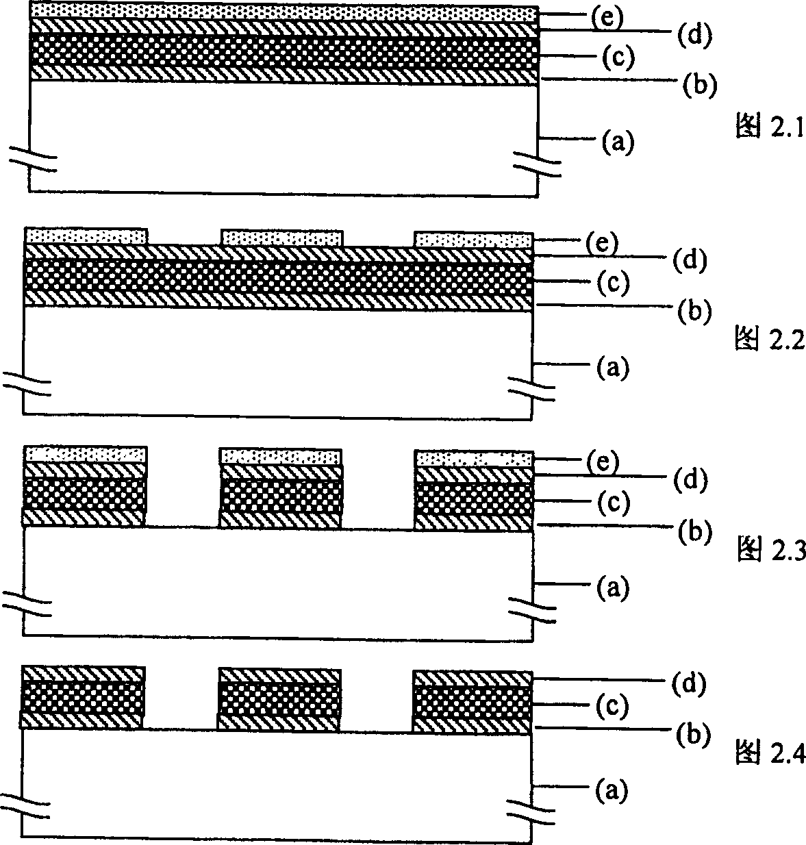
[0050] A scheme of the method of the present invention, such as Figure 5 Shown as:

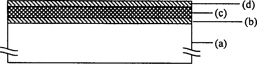
[0051] First, a photoresist mask layer is formed on an anisotropic magnetoresistance (AMR) film. Described anisotropic magnetoresistance effect (AMR) film is the multilayer film that is made up of transition layer / permalloy / protective layer, and a kind of commonly used multilayer film is tantalum (Ta) / permalloy (NiFe) / tantalum (Ta).

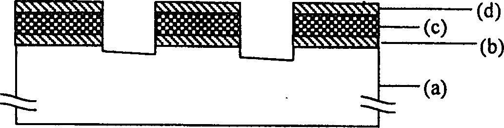
[0052] Next, using the photoresist mask layer as a mask, dry etching is used to etch the protective layer i...


PUM


Abstract

The present invention relates to combined dry and wet etching process for multilayer film, especially in anisotropic magnetic resistance effect (AMR) sensor manufacture. The process includes dry etching the protecting layer of AMR film; wet etching the permalloy (NiFe) layer of the AMR film; and dry etching the transition layer of the AMR film. The AMR film is multilayer Ta / NiFe / Ta film. Compared with traditional technology, the present invention has the advantages of shortened etching time, raised etching efficiency, regular edge of resistance stripes and high graph quality.

Description

technical field [0001] The present invention relates to the etching method of multilayer film (in this application document, dry etching and wet etching are collectively referred to as etching), especially the permalloy used in the manufacture of anisotropic magnetoresistance (AMR) sensor Etching method of multilayer film formed by NiFe) and tantalum (Ta). Background technique [0002] Since the anisotropic magnetoresistance effect (AMR) film can be used to prepare highly integrated devices, sensors based on this effect have a very wide range of uses, such as high-density magnetic heads of hard disks, magnetic encoders, electronic compasses, dynamic vehicle target acquisition and current sensors. Wait. Anisotropic magnetoresistance (AMR) thin films have simple structure, relatively easy fabrication, low price, and good stability, and have great advantages in volume, quality and cost. Even after the discovery of giant magnetoresistance (GMR) and its products Today, hard dis...

Claims


Application Information

Patent Timeline
Patent Type & Authority Applications(China)
IPC IPC(8): G11B5/39H01L43/12
Inventor 高晓光李建平何秀丽
Owner INST OF ELECTRONICS CHINESE ACAD OF SCI
Why Eureka
Try Eureka