

Three-pole carbon nano tube field emission flat display with ballast resistor structure and fabrication process thereof
A flat-panel display and ballast resistor technology, applied in the manufacture of electrode systems, manufacture of discharge tubes/lamps, discharge tubes, etc., can solve the problems of not getting a perfect solution and reducing the brightness of pixels, so as to improve the production success rate, The effect of reducing the emission current and avoiding the difference in thermal expansion coefficient
- Summary
- Abstract
- Description
- Claims
- Application Information
AI Technical Summary
Problems solved by technology
Method used
Image

Examples
Embodiment Construction
[0051] The present invention will be further described below in conjunction with the accompanying drawings and embodiments, but the present invention is not limited to these embodiments.
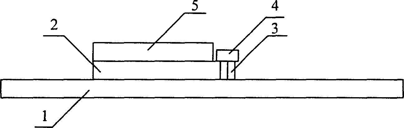
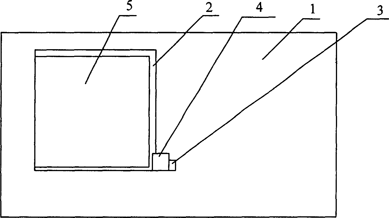
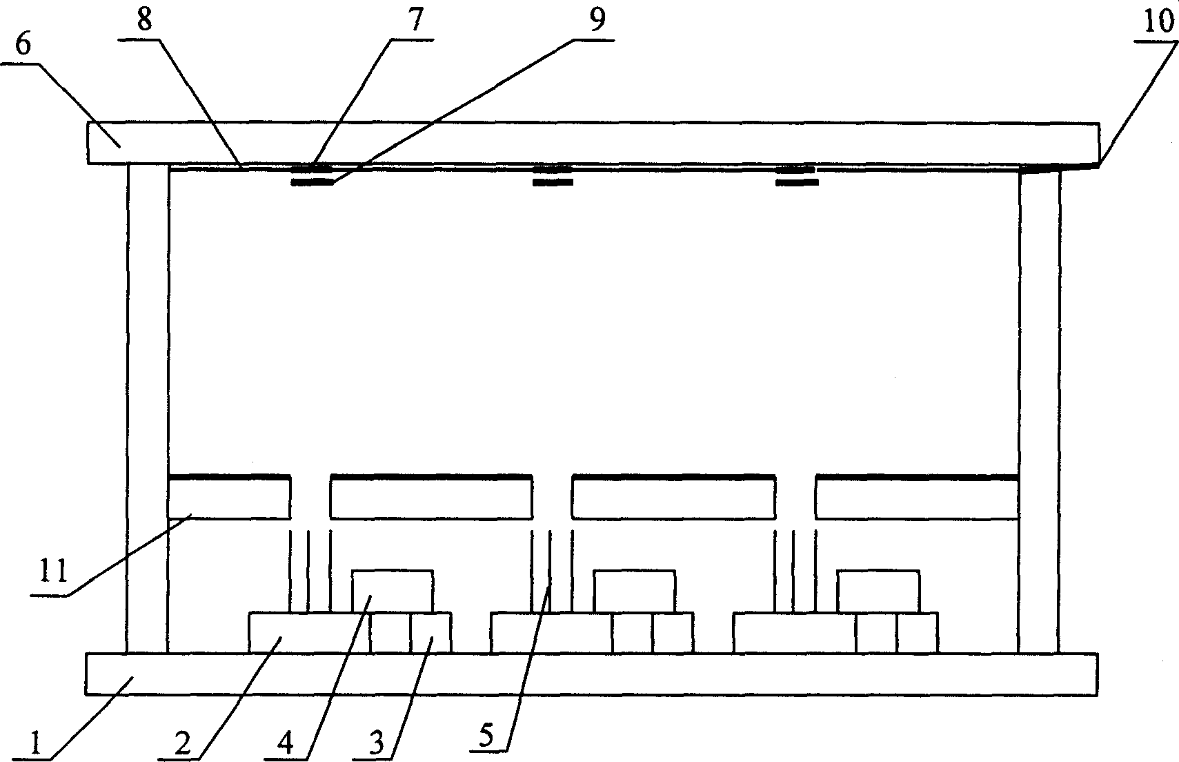
[0052] like figure 1 , 2 , 3, including a cathode panel, an anode panel and a sealed vacuum chamber formed by a glass frame, an indium tin oxide thin film conductive layer 7 and a phosphor layer 9 are arranged on the anode panel, and a control grid 11 is placed on the cathode panel A carbon nanotube cathode conductive layer 2 , a ballast resistor layer 4 and a carbon nanotube cathode 5 are prepared, and a ballast resistor is provided on the corresponding carbon nanotube cathode under each pixel. A ballast resistor is prepared for the corresponding carbon nanotube cathode under each pixel, which is used to adjust the ability of carbon nanotube field emission electrons, so as to achieve the effect of uniform and stable emission of electrons by the overall carbon nanotube cathode. The image d...
PUM
 Abstract
Description
Claims
Application Information